Transparent and conducting IGZO thin films were deposited by RF magnetron sputtering on thin Cu coated glass substrates to investigate the effect of a Cu buffer layer on the structural, optical, and electrical film properties. Although X-ray diffraction (XRD) analysis revealed that both the IGZO single layer and IGZO/Cu bi-layered films were in the amorphous phase, the IGZO/Cu films showed a lower resistivity of 5.7×10⁻⁴ Ωcm due to the increased mobility and high carrier concentration. The decreased optical transmittance of the IGZO/Cu films was also attributed to a one order of magnitude higher carrier concentration than the IGZO films. From the observed results, the thin Cu layer is postulated to be an effective buffer film that can enhance the opto-electrical performance of the IGZO films in transparent thin film transistors.
There is considerable interest in using Al-doped ZnO films [1] and In- and Ga- doped ZnO (IGZO) films as transparent, conducting oxide (TCO) electrodes for transparent electronic devices because of their high optical transmittance in the visible wavelength range, chemical stability, and lower cost of production compared to conventional ITO films [2,3].
Recently, IGZO films have been used as an active layer in transparent thin film transistors (TTFTs) because the films can be deposited as a uniform amorphous phase while retaining high carrier mobility [4]. However, relatively high substrate temperatures are required to produce IGZO films with the required optical and electrical properties for specific applications [5]. One way to enhance the opto-electrical performance of IGZO films, without substrate heating or post-deposition annealing, is to adopt a TCO buffer layer under the IGZO film.
In a previous study, Kim et al. reported that an optimized 10 nm thick Sn doped ZnO (ZTO) buffer layer in the IGZO films enhanced mobility and yielded relatively high optical transmittance without intentional substrate heating [6].
In the current study, IGZO/Cu bi-layered films were deposited by radio frequency (RF) and direct current (DC) magnetron sputtering on glass substrates. Cu film is a superb conductor with an enormous carrier concentration and is used as a buffer layer for IGZO films to enhance the opto-electrical performance in TTFT applications.
For these reasons, we investigated the impact of a 5 nm thick Cu buffer layer on the structural, optical, and electrical properties of the IGZO/Cu films using X-ray diffraction (XRD), atomic force microscopy (AFM), Hall-effect measurements, and UV-Visible spectrophotometry.
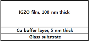
Prior to deposition, the deposition chamber was evacuated to 3×10⁻⁴ Pa and the distance between the targets and substrates was maintained at 60 mm. Thin Cu films with a thickness of 5 nm were deposited onto glass substrates (Corning 1797, 3×3 cm2) using a Cu target and DC magnetron sputtering. Subsequently, 100 nm thick IGZO films were deposited onto the Cu buffer layer by RF magnetron sputtering using an IGZO target with an atomic ratio of In: Ga: Zn of 0.33: 0.33: 0.33, respectively and 3-inch diameters without intentional substrate heating. Glass substrates were degreased in a dilute detergent solution, rinsed in deionized water, and blown dry in nitrogen gas before they were set on the substrate holder in the chamber. Figure 1 shows the schematic diagram of IGZO/Cu bi-layered films and Table 1 lists the experimental conditions used for this study.
[Table 1.] Experimental conditions of RF and DC magnetron sputtering.
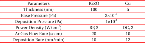
Experimental conditions of RF and DC magnetron sputtering.
After deposition, film thickness was confirmed using a surface profiler (Dektak-150, Varian), and the crystallinity of films was investigated by XRD (X’pert PRO MRD, Phillips) analysis at the Korea Basic Science Institute (KBSI, Daegu center). Optical transmittance in the visible wavelength region was determined using a UV-Vis spectrophotometer (Cary 100 Cone, Varian). The bare glass substrates exhibited an optical transmittance of 91%. Variations in surface morphology (2×2 μm2 scanning area) and root mean square (RMS) roughness of the films were characterized by atomic force microscopy (AFM, XE-100, Park Systems). Electrical properties of the films were investigated by Hall Effect measurements employing the Van der Pauw technique (HMS-3000, Ecopia).
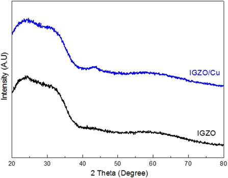
Figure 2 shows the XRD patterns of an IGZO single layer and IGZO/Cu bi-layered films. Regardless of the Cu buffer layer, all of the films showed a broad peak between 20° and 40°. No diffraction peak could be ascribed to the crystalline phase of the IGZO and Cu films. Recently, Cho, et al. reported that when the annealing temperature was below 600℃, no crystalline peaks were present in the XRD pattern of IGZO films [7]. Based on these previous reports and the XRD patterns shown in Fig. 1, crystal growth did not appear to occur for IGZO/Cu films without intentional substrate heating.
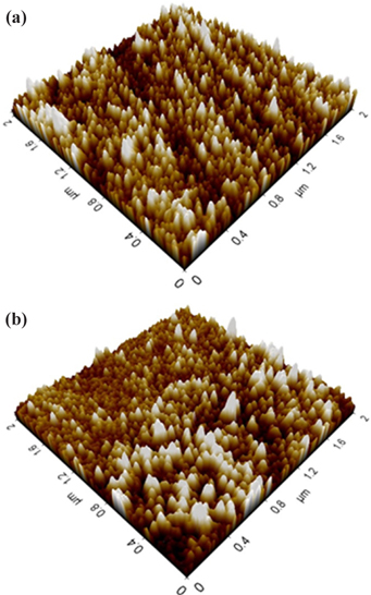
Figure 3 shows the surface morphologies of the IGZO single layer and IGZO/Cu bi-layered films. The surface morphology of TCO films is an important determinant of the optical and electrical properties. The as-deposited IGZO films had an RMS roughness of 1.79 nm, while the surfaces of IGZO/Cu films were smoother, and the RMS roughness having decreased to 1.32 nm. The presence of a Cu buffer appeared to enhance the flatness of the upper IGZO films, indicating the Cu film grew preferentially in the sunken regions of the substrate during buffer layer deposition and, conferring a flatter surface than the single layer IGZO films. In a previous study, Chae et al. reported similar results with respect to the surface morphology of ITO/Cu bi-layered films prepared by RF and DC magnetron sputtering. The roughness of the upper ITO films also decreased by the presence of a Cu buffer layer [8].
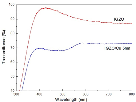
Figure 4 shows the optical transmittance spectra over the visible wavelength region for the as-deposited IGZO single-layer and IGZO/Cu bi-layered films. After insertion of the 5 nm thick Cu buffer layer, the optical transmittance of the IGZO films decreased from 92.2% to 72.2%. The optical transmittance of TCO/metal bi-layered films is widely known to be affected by light absorption due to inter band electronic transitions; these transitions are a result of electron excitation from the d-band to the Fermi surface [9]. Table 2 shows the electrical properties for the IGZO single layer and IGZO/Cu bi-layered films. The IGZO/Cu films had carrier concentrations two orders of magnitude higher (1.0×1021 cm-3) than the IGZO single layer films. Thus, there were more bound electrons available for excitation, which in turn decreased the optical transmittance in the visible wavelength region. The absorption edges in the optical transmittance spectra were shifted towards a longer optical wavelength. A similar red-shift of the absorption edge was reported in a previous study of ITO/Au bi-layered films [10], as well as an increased carrier concentration as shown in Table 2.
[Table 2.] Electrical properties of IGZO single layer and IGZO/Cu bilayered films.
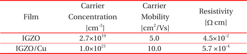
Electrical properties of IGZO single layer and IGZO/Cu bilayered films.
The figure of merit (FOM) is an important index used to evaluate the performance of TCO films. The FOM is defined as:
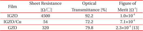
where T is the optical transmittance in the range of visible wavelengths and Rs is the sheet resistance of the film [11,12]. Table 3 shows a comparison of the FOM values for GZO, IGZO and IGZO/Cu bi-layered films [13]. By insertion of 5 nm thick Cu thin films as a buffer layer of IGZO film, the FOM increased to as high as 7.1×10⁻⁴ Ω−1 for IGZO/Cu bi-layered films. A larger FOM is indicative of better optical and electrical performance of a TCO film, and thus we concluded that the IGZO/Cu films prepared in this study performed better than films annealed at other temperatures.
[Table 3.] Figure of merit of GZO, IGZO single layer and IGZO/Cu bilayered films.

Figure of merit of GZO, IGZO single layer and IGZO/Cu bilayered films.
Both IGZO single layer and IGZO/Cu bi-layered films were deposited on glass substrates using RF and DC magnetron sputtering without intentional substrate heating to investigate the effects of the Cu buffer layer on structural, electrical, and optical properties of the IGZO/Cu films. The IGZO/Cu films had a carrier concentration that was one order of magnitude larger than that of the IGZO films, suggesting that the Cu buffer layer decreased the resistivity of IGZO films to as low as 5.7×10⁻⁴ Ωcm without intentional substrate heating.
Finally, the IGZO/Cu films exhibited a figure of merit of 7.1×10⁻⁴ Ω−1, seven times higher than the IGZO films. Since a higher figure of merit is indicative of improved optical and electrical performance of TCO films, the IGZO/Cu films was concluded to have better opto-electrical performance properties compared to the IGZO films.