As increasing demands for multi-function mobile consumer electronic devices, the complexity of the interconnection density of semiconductor chips continuously increase. Conventional chip to packaging integration (CPI) uses wire-bonding for interconnection of bonding pad to package leads. As chip scaling moves towards the atomic level, chip-to-chip interconnections using through silicon via (TSV) technology become an attractive potential solution for enabling higher performance form factors with low manufacturing cost [1]. Vertical electrical interconnects that pass through the silicon die can reduce the lengths of chip-to-chip interconnections and enable more compact CPI interconnection structures [2,3]. In TSV fabrication, high aspectratio structures with controlled sidewall profiles in silicon are important for microelectronic devices in the nanometer and micrometer scale [4].
TSV interconnection technology consists of deep silicon etching for via formation, insulating liner layer deposition, and via filling with conductive metals. Vertical and deep silicon via etching is attainable by plasma etching, but is still a challenging and complex fabrication process. Deep silicon via etching requires highly energetic ion bombardment to deliver enough kinetic energy to break chemical bonds of the silicon atoms on the wafer and immediate chemical reactions of highly reactive radicals to form a volatile etch by-products. Ion charging in a deep via region may cause a localization of silicon etching. Reactive radicals can increase the etch rate of silicon via, but it also increases lateral etch rate of TSVs. Increased ion bombardment can cause the erosion of via etch mask, and poor quality etch masks can result rough sidewall profiles [5]. Recent investigation employed hydrocarbon and hydro-fluorocarbon (HFC) gas chemistry to improve TSV etching profiles by forming a sidewall passivation and prevent etch mask erosion [6].
In this research, we investigated the effect of different types of etch mask in TSV etch and the effect of the sidewall profiles in TSVs. We first examined the sidewall profiles of TSV with a conventional photoresist (PR) mask, and investigated the effects of two types of hard masks on the sidewall profile of TSVs. The investigated TSV etch materials are photoresist, silicon dioxide, and aluminum. With narrower pattern sizes of masks, the etch depth and the etch rate tend to decrease.
Known as aspect-ratio-dependent-etching (ARDE), this result is suspected to be primarily dependent on ion shadowing. When a soft mask had been used, scallop collapse of sidewall occurred below 6 μm as shown in Fig. 2.
Interaction between photoresist erosion and ion angular dispersion within sheath causes this abnormality. In contrast, no abnormalities occurred when hard masks were used. Etch rate and selectivity of the hard mask were superior compared to the soft mask. We recommend use of hard masks for finer TSVs and to reduce the amount of undercut and collapsed scallops.
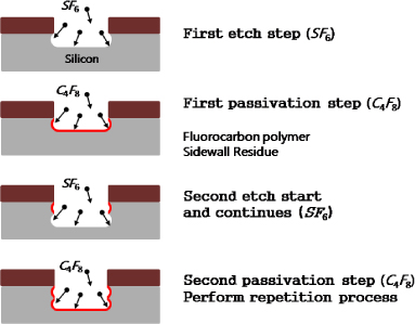
Traditional plasma etching may suffer from a difficulty in high-aspect-ratio via etching, but the deep reactive ion etching (DRIE) with the Bosch process alleviated the concerns in TSV etching [8]. The Bosch process is performed by alternating passivation and etching steps, and is known as gas chopping etching or time multiplexed deep etching.
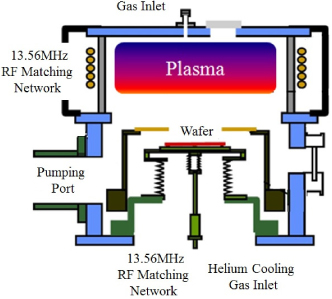
Figure 1 shows a schematic of typical Bosch process for deep silicon etching using
Samples for TSV fabrication were prepared on 4 inch <100>
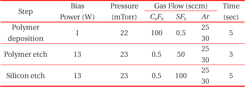
Table 1 shows the process recipe including gas mixture used in this experiment.
[Table 1.] TSV etch recipe (source power was fixed at 825 W).

TSV etch recipe (source power was fixed at 825 W).
Results of the etch profile using three different etch masks: photoresist, oxide, and metal. Factors considered for the evaluation of different types of etch mask are undercut, scallop, and etch rate.
3.1 Photoresist mask (Soft mask)
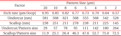
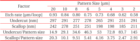
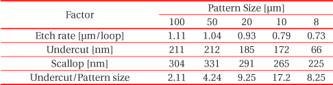
AZ 1512 photoresist was used for etch mask material, overall via etch results are presented in Table 2. Etch rates are monotonically decreased with the decrease in the size of diameters of TSVs, and is explained as the aspect ratio dependent etching (ARDE) in plasma etching. No significant amount of undercut was observed in larger vias, but undercut was drastically decreased in 8 μm sized vias. When the ratio of the amount of undercut and the pattern size was considered, smaller sized vias had much larger ratios of undercut to pattern size. This called our attention and led to further investigation of the etch profile in TSV for smaller pattern sizes with different mask materials.
[Table 2.] TSV etch profile using AZ 1512 photoresist etch mask.
TSV etch profile using AZ 1512 photoresist etch mask.
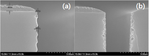
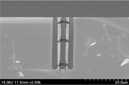
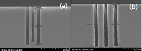
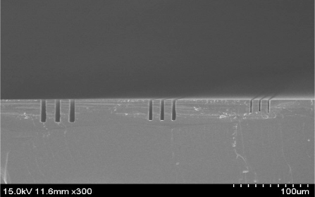
Successful TSV profile was achieved in via sizes larger than 10 μm, but collapsed scallop patterns were observed below 10 μm size TSVs. Figure 4(a) shows via etching result in 8 μm sized via, and collapsed scallops began at the top of sidewall. As shown in Fig. 4(b), increased amount of collapsed scallops were observed in smaller sized vias. The scallop collapse has not been found in experiments using hard masks that will be described later.
Photoresists are useful etch mask materials for TSVs in larger diameter diameters, but may not suitable for smaller sized vias for collapsed scallops. To further investigate alternatives to photoresists for smaller sized TSV patterning, we investigated hard mask materials. The first candidate is silicon dioxide (
[Table 3.] Etch result of using SiO2 mask.

Etch result of using SiO2 mask.
In terms of silicon etch rate employing silicon dioxide hard mask, it was successfully demonstrated a potential of TSV etch mask down to 3 μm diameter TSVs. We observed non-uniformly etched TSV profiles in a 2 μm diameter TSV, which is known as the loading effect [9] and is presented in Fig. 5(a). Etch rate uniformity deteriorates when pressure or average loading increase [10], and Argon does not chemically reacted with the poly and removes the passivation layer by sputtering the polymer with high energetic ions [11].
In order to avoid the loading effect due to high energy ions in our experiment, we reduced
Among metal candidates used in semiconductor fabrication, aluminum is often selected for their ease of fabrication and compatibility with conventional fabrication process steps. Aluminum has been widely used for metal interconnections before copper metal interconnection is required for reducing interconnection delay. It is still used for back-end-of-line (BEOL) interconnection and bonding pad in many semiconductor products. Although metal etch masks are not used in conventional semiconductor fabrication processes, we are interested in this durable and reliable etch mask for the successful fabrication of finer features of TSVs. Table 4 shows via etch results with metal hard mask. As the pattern sizes become smaller, ARDE was also observed as shown in the previous experiments with different mask candidates.
[Table 4.] Etch result of using Al mask.

Etch result of using Al mask.
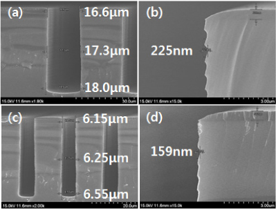
Comparing the etch rates presented in Table 3 and 4, both types of hard masks showed similar etch rates in various sizes of TSVs. Unlike with hard oxide mask, metal masks showed improved undercut and scallop collapse, and the etched profiles are summarized in Table 4. Figure 6 shows TSV etch profiles in 2 μm diameter TSVs.
4.1 Aspect-ratio-dependent-etching (ARDE)
With narrower pattern sizes, the etch depth is observed to decrease as shown in Fig. 7. Silicon etch rate is retarded especially with narrower pattern sizes is known as aspect-ratio-dependentetching (ARDE) [12] or reactive ion etching (RIE) lag [13,14]. Although there are many factors of RIE lag, ARDE can be explained by three main reasons: ion shadowing, neutral shadowing, differential charging. Ion shadowing means the loss of ion flux at the bottom of the etched structure [12], neutral shadowing is caused by the depleted reactive neutral species in plasma [14,15], and differential charging which describes a tendency in which the top of pattern and top of sidewall is negatively charged and the bottom surface is positively charged if aspect ratio is higher [16]. In this experiment, we postulate that ion shadowing is the main reason for the observed ARDE. DRIE uses high-energy ion bombardment from plasma to attack the wafer surface and reactant gas species to chemically react with the surface material [17]. The loss of etchant species
4.2 Photoresist erosion & ion angular dispersion
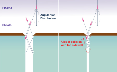
Soft masks in pattern sizes below 10 μm lead to collapsed scallops. In comparison, hard masks can yield a pattern up to 2 μm and can provide the better etch results than the soft masks. In this section, we describe the reasons of this phenomenon. Initially, collapsed scallops were thought to result from difference of substance between soft masks and hard masks. The photoresist soft mask is made up carbon-hydrogen bond, and the collapsed scallop were assumed to occur by reaction to carbon-hydrogen from the bond breaking polymer material by plasma [21,22]. If bond breaking of polymer material was cause of the collapsed scallop, sidewalls of whole pattern range under the photoresist mask must collapse similarly. For example, via pattern over 10 μm were successful as Fig. 8 but not below 10 μm. We noted two features in the collapse of scallop that started from top of sidewall and the thin form of photoresist mask on top edge of sidewall as in Fig. 8. The photoresist erosion is due to the formation of faceting angels on the top edge of patterns by high density ion plasma etch [23].
The start of the collapsed scallop from the top and photoresist erosion appeared to be related. In thinner photoresist masks both energy transmittance of mask and normalized focus range are increased [24,25]. This is why sidewall under thin photoresist mask has more damage rather than original thickness. Secondly, the cause of the defects of sidewall is the angular dispersion of ions by collisions with the sheath [26]. As the pattern narrows when the sidewalls get closer together, the number of ion collisions with sidewall increases at the top of the sidewall. The top sidewall receives more damage and the sidewall surface defects were created. The angular dispersion of ions is depicted in Fig. 9. This defect affects subsequent steps.
Since the sidewall surface defects were created during the previous etch steps, poor fluorocarbon polymer coverage on sidewall is created during passivation step. Poly-tetra-fluoroethylene (PTFE) is used to prevent lateral etching during severe etching [27]. If the sidewall surface becomes rough during the etch step, to deposit a polymer on sidewall as next step will fail, and it will get worse over and over again [28]. So in this research, collapsed scallop appears from the use of photoresist mask of narrow pattern. To solve this problem, mask thickness has to be increased. But thicker photoresist masks are prone to cracking as well as a large amount of photoresist have to be used [29]. On the other hand, silicon oxide mask and aluminum mask as hard mask endured plasma damage including ion bombardment. So there were not collapsed scallop on sidewall and there became good profile until 2 μm pattern in using hard masks. Also in this research, we confirmed that selectivity of hard mask is higher than soft mask.
In this experiment, we investigated etch mask materials for the fabrication of finer sized through silicon vias (TSVs). Conventionally employed photoresist used as silicon etch masks may not be suitable for finer features of TSV fabrication using the Bosch process, and we suggested the use of hard masks for finer TSVs to reduce the amount of undercut and collapsed scallops. Hard metal masks in aluminum provided superior sidewall profiles of TSVs as small as 2 μm in diameter. Hard mask of silicon dioxide was useful in fabricating TSVs smaller than 20 μm, down to a few micro-meter diameters, but concerns of undercut below the oxide mask remain. Regardless of etch hard mask materials, ARDE from ion shadowing was observed.
![Principle of deep reactive ion etching (DRIE- Bosch) process [7].](http://oak.go.kr/repository/journal/20737/E1TEAO_2015_v16n6_312_f001.jpg)