Thin film transistors (TFTs) based on amorphous oxide semiconductor (AOS) have been recently studied due to their high electrical properties and transparency in the visible region. Recently, many studies were reported high performance of the zinc oxide based TFTs. The amorphous indium-gallium-zinc-oxide (a-IGZO) is the one of the most famous channel materials in AOS TFTs. a-IGZO TFTs demonstrated high field effect mobility (>10 cm2V−1s−1) [1-4]. However, indium is an expensive and rare material. Therefore, many potential alternative materials were studied to replace the expensive indium [5]. The zinc-tin-oxide (ZTO) has been steadily researched over the past few years [6,7].
In our previous work, Si doped ZTO channel showed enhanced electrical properties compared with the traditional a-I GZO channel [8]. The transmission line method (TLM) is used for the evaluation of sheet resistance, contact resistance, and total resistance between the channel and source/drain electrodes [9,10]. Improvement of electrical properties requires low specific contact resistance and good ohmic contact.
In previous studies, many electrode materials, such as Ti, Al, Pt, and Au have been selected for testing ohmic contact to n-type ZnO [11]. It is important to improve the contact resistance between the source/drain and channel layer to enhance device properties, such as the field effect mobility, which determines device performance, as well as the subthreshold slope (S.S) and switching speeds [12].
In the present study, we report the effect of different source/drain electrodes (Al and Ti/Al) on the contact resistance of the interface between the source/drain electrodes and the channel by using the TLM pattern.
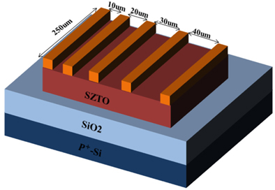
The SZTO layer (SZTO target; 0.5 wt.% Si doped ZTO (Zn:Sn=65:35) was deposited onto a SiO2/p-type Si substrate at room temperature by radio frequency (RF) sputtering, supplying a power of 30 W, an Ar/O2 (30/0) atmosphere, and a working pressure of 2 mtorr. The thickness of the channel layer is approximately 40 nm. For the TLM, the channel width (250 μm) and lengths (ranging from 10 μm to 40 μm) were used. For TFTs, the width/length was fixed at 250 μm/50 μm. After deposition, the film was post annealed for 2 hours at 500℃, after which different electrodes were deposited and followed by the lift-off processes. The Ti (10 nm) and Al (50 nm) as source/drain electrodes were deposited using an e-beam and thermal evaporation, respectively.
Figure 1 shows a schematic diagram of the bottom gate a-0.5SZTO TFTs with TLM patterned. The contact resistance and TFTs characteristics were measured using the semiconductor parameter analyzer.
The total resistance measured in each of the TLM configurations is a function of the contact resistance at the channel/electrodes interfaces and the sheet resistance of the channel. The total resistance can be calculated by using the equation (1) [9].

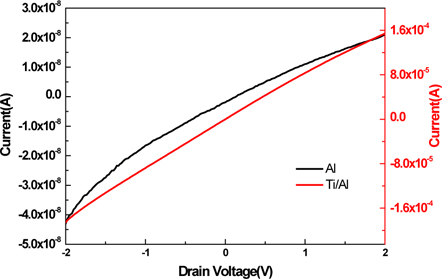
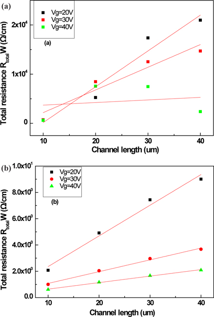
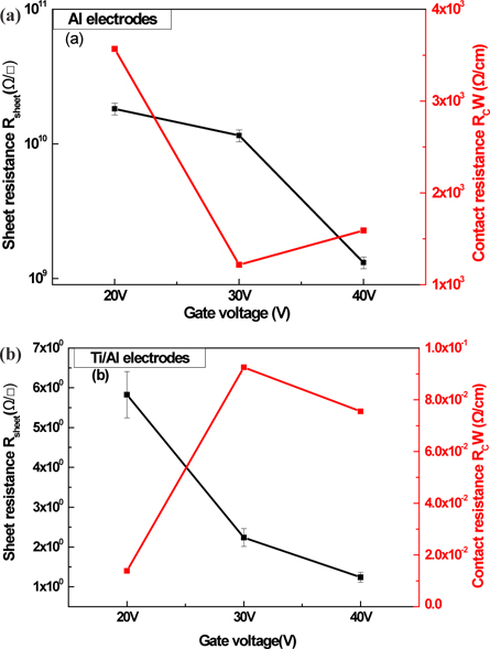
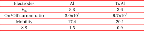
where, d is the separation of the electrodes, Rcontact is the contact resistance between the channel and the S/D electrodes, Rtotal is the total resistance, Rsheet is the sheet resistance of the semiconducting layer outside the contact, and W is the fixed electrode width of 250 μm. In the present study, the TLM characteristic of a-0.5SZTO TFTs measured at gate voltage (Vgate)=40 V and drain voltage (VDS) was swept from −2 V to 2 V. The Al electrode of a-0.5SZTO TFTs showed non-ohmic contact and current was generally 10−8 A. On the other hand, the Ti/Al electrodes of a-0.5SZTO TFTs showed ohmic contact and the current was recorded at 10−4 A, as shown in Fig. 2. Table 1 shows the work functions of a-0.5SZTO and other metals. The work function of Ti is approximately 4.33 eV and for Al approximately 4.06~4.26 eV [14]. We measured the work function of a-0.5SZTO using a Kelvin probe. The work function of a-0.5 SZTO showed approximately 4.53 eV. Low work function differences could be due to decreased barrier height between the channel and electrodes interface, allowing carriers to move more easily. Ti/Al electrodes of a-0.5SZTO TFTs showed a smaller work function gap than did the Al electrode. The relationship between Rtotal and channel length (Lch) with the Al electrode, and Ti/Al electrodes are shown in Fig. 3. As the Rtotal increases, Lch is also increased. a-0.5SZTO TFTs with Ti/Al electrodes (Fig. 3(b)) demonstrated low Rtotal compared with that of the Al electrode (Fig. 3(a)) since the a-0.5SZTO TFTs with Ti/Al electrodes had a Rtotal less than 1.0×10² Ω/cm while TFT with Al only electrode showed Rtotal greater than 102 Ω/cm. A possible explanation for this result is that Ti may improve the contact between the channel and the electrodes. Figure 4 shows the Rcontact and Rsheet based on Vgate with the Al electrode, and Ti/Al electrodes. It is clear that the Rsheet was reduced from 1010 (Al electrode) to 100 Ω/sq (Ti/Al electrodes) at Vgate= 30 V, and Rcontact was also reduced from 103 to 10−2 Ω/cm at Vgate= 30 V.
[Table 1.] Work function values for a-0.5SZTO and other metals.
Work function values for a-0.5SZTO and other metals.
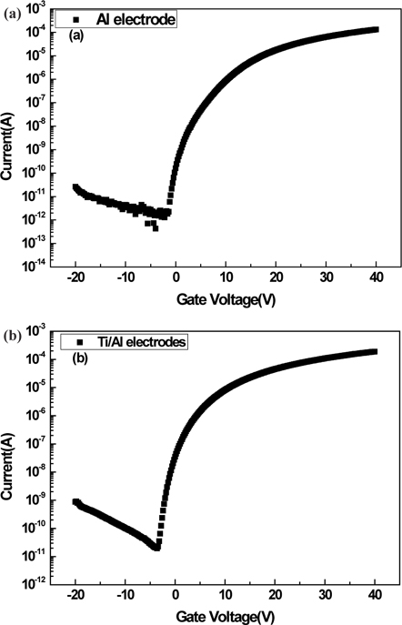
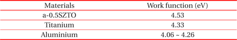
Figure 5 demonstrates the transfer curve of a-0.5SZTO TFTs with Al electrode, and Ti/Al electrodes. The electrical properties can be calculated by equation (2).

where, VDS is drain voltage, gm is the transconductance, Cox is the oxide capacitance of the gate insulator, W and L are channel width and length. We fixed the VDS at 5.1 V for calculating the drain current. The electrical properties, such as Vth, Ion/off, μFE, and S.S are summarized in Table 2. The a-0.5SZTO TFTs with Ti/Al electrodes showed higher current level (10−11 A) than Al electrode (10−13 A) because the Al showed Schottky contact. In previous studies, Schottky contact improved leakage current characteristics. On the other hand, Ti/Al electrodes show ohmic contact due to Ti enhanced contact characteristic such as contact resistance at the interface. Thus, Ti/Al electrodes show better performance than Al. The TFTs with Ti/Al electrodes μFE of 20.1 cm2 V−1s−1, S.S of 0.9 V decade−1, and Vth of 2.6 V have been obtained. On the other hand, TFT with Al electrode showed the μFE of 17.4 cm2 V−1s−1, S.S of 1.5 V decade−1, and Vth of 8.8 V. This result could be obtained since Ti/Al electrodes showed good ohmic contact, low Rcontact, low Rtotal, and low Rsheet compared with that of the TFT with the Al only electrode.
[Table 2.] The TFTs characteristic of a-0.5SZTO thin film with different electrodes.
The TFTs characteristic of a-0.5SZTO thin film with different electrodes.
In summary, we fabricated a-0.5SZTO TFTs and compared the Al only electrode with the Ti/Al electrodes. We have measured the Rtotal using the TLM patterns. It is clear that the Rtotal with Ti/Al was less than that of the Al electrode. This could be expected due to Ti. Ti can improve contact characteristics between channel layers and electrodes. This is clearly demonstrated by TLM in this study. TFTs with Ti/Al showed good performance compared with the TFT with Al only electrode. The μFE of 20.1 cm2 V−1s−1, S.S of 0.9 Vdecade−1, and Ion/off of 9.7×10⁶ A have been obtained from TFT with Ti/Al electrodes.