Given the emerging threats of resource depletion and environmental challenges of the 21st century, many researchers have begun actively studying sources of renewable energy. Recently, solar energy has gained much attention for this purpose. Solar energy application using photo-thermal conversion is the most important factor in order to prepare a solar selective absorber and choose materials with higher efficiency [1-4]. The important qualities for solar absorber coatings are high absorptance and low reflectance in the solar spectral range of 0.3~2.5 μm. The thermal absorber can convert low solar energy density to high heat energy density, improving the efficiency of photo-thermal conversion [5]. The most widely used solar selective materials, proposed by Granqvist in 1978 [6], are cermet absorbers, such as Pt-Al2O3, Mo-Al2O3, and Ni-SiO2 with thermal stability at high temperatures exceeding 400℃. Recently, transition metal nitrides or oxynitrides have attracted interest due to excellent chemical, microstructural and optical properties. The binary nitrides AlN and CrN with wurtzite and rock salt crystal structures have low solubility in the thermal equilibrium at high temperature. This problem can be overcome by PVD (physical vapor deposition) methods with the formation of metastable solid solutions in crystallographic modifications of binary systems, where Al and Cr atoms are substituting each other [7-10]. It is known that TiN and TiAlN exhibit high absorptance in the solar spectral range and low emittance in the deep infrared region. The crystal structure of CrN and TiN provide good electrical conductivity, thermal stability, and high hardness [11-13]. Magnetron sputtering is suitable for growth of epitaxial single layers in the binary systems of TiN, AlN and CrN. The magnetron sputtering has some merits in comparison with other deposition methods. Firstly, the sputtering deposition is a widely used method for coating a large area of solar material. Secondly, the method is adaptable to various kinds of thin film materials such as metals, oxides, nitrides, organic materials, and ceramics. Thirdly, the reactive sputtering using the metal target can easily control the binary film composition with components and contents of gas injection. Lastly it has the advantage of gaining a high deposition rate, and it is able to regulate the thickness of thin films [14-16].
In the present study, CrN and TiN metal nitride films on aluminum substrate were deposited by the DC reactive magnetron sputtering method. The microstructure and optical characteristics of the solar absorber CrN/TiN/Al with differences in N2 gas rate were investigated. The crystallinity and surface properties were estimated by X-ray diffractometer (XRD) and field emission scanning electron microscophy (FE-SEM). The exact composition and optical properties of thin films were measured by Auger electron spectroscophy (AES) and UV-Vis-NIR spectrophotometer.
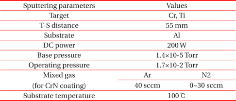
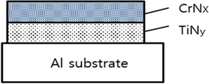
DC reactive magnetron sputtering system with multi targets was used for the solar selective coating. The Cr and Ti targets with purity of 99.9% was sputtered in Ar (99.99%) and N2 (99.99%) mixed gases. The solar absorber films were deposited under the base pressure of 1.4×10⁻⁵ Torr and operating pressure of 1.7×10⁻² Torr. The flow rates of Ar and N2 gases, which served as the sputtering atmosphere, were controlled separately by mass flow controllers. The top layer of CrN as shown in Fig. 1 was used with an Ar gas flow rate of 40 sccm and N2 gas ranges of 0~30 sccm. The TiN layer was prepared used Ar gas of 40 sccm and N2 gas of 10 sccm. The substrate temperature was kept constant at 100℃. The deposition parameters of the multi-layer solar selective absorber coating are listed in Table 1. The gas mixture of Ar and N2 with a variation rate of N2 was the important parameter for sputtering deposition and the solar absorber coating. Therefore, the metal volume fraction (MVF) was controlled by N2 gas flow rate on the binary nitride films. The microstructural properties of absorber films with different MVF values were examined.
[Table 1.] Sputtering conditions of as-deposited solar absorber films.

Sputtering conditions of as-deposited solar absorber films.
A schematic diagram of the CrN/TiN/Al multi-layer absorber structure is shown in Fig. 1. The crystallinity of the resulting films was assessed by X-ray diffraction, using CuKα radiation in the range of 2 Θ=10~90°. The surface and material properties were estimated by FE-SEM, atomic force microscopy (AFM) and AES. The absorptance of the thin films were measured at the wavelength ranges of 0.3~1.1 μm by Hitachi UH4150 UV-Vis-NIR spectrophotometer. Solar absorptance of the multi-layer was calculated using standard AM1.5 solar spectrum.
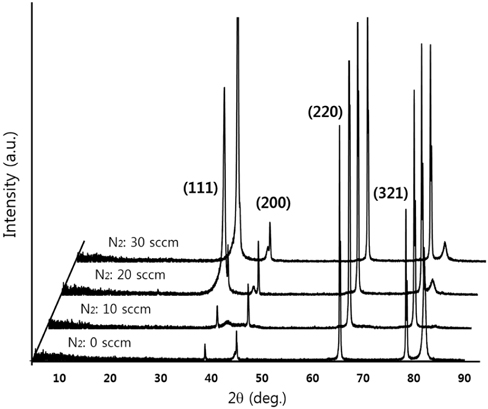
Figure 2 shows XRD patterns of the CrN/TiN/Al binary nitride thin films at different N2 gas flow rates during CrN deposition. As the N2 flow rate was increased to 30 sccm, the MVF of the top layer of CrN film changed from high metal volume fraction (HMVF) to low metal volume fraction (LMVF). The high intensity peak centered at 2 Θ=65.34° and other weaker peaks at 2 Θ=38.74°, 44.96°, and 78.45° are demonstrated in Fig. 2. The strong peak of 2 Θ=65.34° can be attributed to the (220) plane, and other peaks are due to the (111), (200) and (321) planes, respectively. The peak at 2 Θ=38.74° increases abruptly with the increasing flow rate of N2 gas from 10 sccm to 20 sccm. In addition, the peaks at 2 Θ=44.96° and 78.45° increase gradually with the increasing flow rate of N2 gas. As the CrN layer changed from HMVF to LMVF, the crystallinity of the films increased.
[Fig. 2.] XRD patterns of CrN/TiN/Al multi-layer at different flow rate of N2 gas during CrN growth.

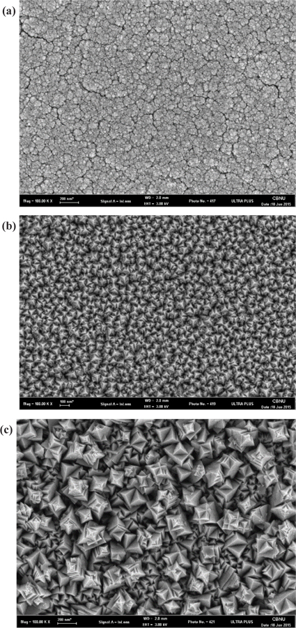
FE-SEM images of the CrN/TiN/Al binary nitride thin films at different N2 gas flow rates during CrN deposition are shown in Fig. 3. The surface image of Fig. 3(a) shows that majority is composed of large irregular coarse particles and the surfaces shown in Fig. 3(b) and (c) clearly change into crystalline pyramid-like grains. For these reasons, the crystallinity is attributed to the preferred growth along the (111) direction as shown in the XRD results of Fig. 2 with the increasing flow rate of N2 gas from 10 sccm to 20 sccm.
As seen in the resulting FE-SEM images, the grain size of thin films with increasing N2 gas flow rate increases gradually. This closely matches the crystalline property of films as shown in the XRD results of Fig. 2. Based on these findings, it is concluded that Cr has been nitridized with increasing N2 flow rate.
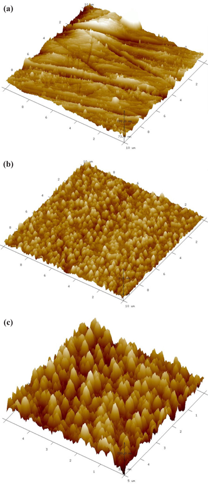
Figure 4 illustrates the three dimensional atomic force microscopy (AFM) images of the surface roughness of each layer in the CrN/TiN/Al multi-layer absorber. The root mean square (RMS) roughness values of the Al substrate, TiN layer, and the as-deposited CrN layer were 4.56, 10.8, and 35.5 nm, respectively. The reason that the RMS roughness values are increased with each growing layer in CrN/TiN/Al film is due to the crystallinity of the increasing grain size.
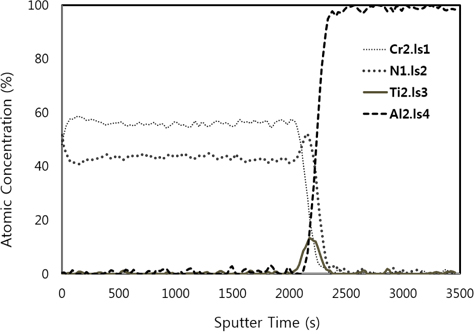
Figure 5 shows the AES depth profile analysis of the CrN/TiN/Al binary nitride film. As the flow rate of nitrogen gas increases, it appears that the peak of nitrogen shows strongly. All peaks of Cr, N, Ti, and Al elements are displayed clearly, because the diffusion in the interface of the CrN and TiN layer and the Al substrate does not occur. Based on the AES depth profile results, the thicknesses of CrN and TiN are approximately 800 nm and 200 nm, respectively.
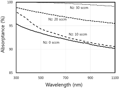
Figure 6 shows the different absorptance spectra of the CrN/TiN/Al absorber films with various flow rates of N2 gas. All absorptance curves of films are recorded above 90% in the the wavelength range of 300~1,100 nm. As the N2 flow rates increase from 0 to 30 sccm, the absorptance also tended to increase.
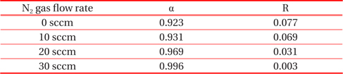
Table 2 displays the absorptance and reflectance values of CrN/TiN/Al films as shown in Fig. 6. The absorptance of binary nitride films with increasing flow rates of N2 tends to increase and, conversely, the reflectance is reduced.

Absorptance and reflectance values of samples with increasing flow rate of N2 gas as shown in Fig. 5.
In the present study, the CrN/TiN/Al multi-layer films of the solar selective absorber were prepared by utilizing a dc reactive magnetron sputtering system with multiple targets. The binary nitride CrN layer deposited with changes in N2 gas flow rates. The XRD results show that the peak of (111) plane at 2 Θ=38.74° increases abruptly with increasing flow rate of N2 gas from 10 sccm to 20 sccm. As the CrN layer with increasing N2 flow rate changed from HMVF to LMVF, the crystallinity of the films increased. From the FE-SEM images, the grain size of films with increasing N2 gas flow rate also gradually increased. These findings are consistent with the crystalline property of CrN/TiN/Al films as shown in the XRD results. The AES depth profile results indicated that all peaks of Cr, N, Ti and Al elements were shown clearly. In addition, the thicknesses of CrN and TiN were confirmed to be approximately 800 nm and 200 nm, respectively. All absorptance curves of the films were greater than 90% in the wavelength range of 300~1,100 nm. As the N2 flow rates increased from 0 to 30 sccm, the absorptance tended to increase and, in contrast, the reflectance decreased.