Grating couplers (GCs) are the most convenient means to couple a light beam between photonic integrated circuits (PICs) and external optical fibers [1, 2]. The silicon-on-insulator (SOI) platform is widely used to form planar integrated photonic devices. Optical input and output beams to and from silicon-based integrated photonic devices mostly require single-mode fibers. However, there is a significant mismatch of the confined optical mode sizes between the optical fiber and silicon waveguide, because a conventional optical fiber has a core size of about 10 micrometers, while the silicon waveguide has a core size of a few hundred nanometers. GCs are simple, easy tools for optical coupling between silicon waveguides and optical fibers, because they can be formed anywhere on the silicon photonic chip for vertical coupling, while the conventional edge coupling of a planar waveguide to an optical fiber requires tapering waveguide ends and antireflective coatings on the ends of the fiber and waveguide.
However, in spite of their beneficial properties, GCs have the one major drawback of limited coupling efficiency, which results in relatively high coupling loss, usually above 3 dB with conventional uniform grating structures. This coupling loss results mainly from the mode mismatch between the fiber mode and the scattered beam profile from the GC, and from the optical beam leakage though the waveguide bottom beneath the GC. The beam profile of the optical fiber core is a Gaussian shape, but the scattered beam profile of the conventional GCs in a uniform grating structure is not Gaussian. Thus the optical loss due to this mode mismatch causes an optical coupling loss larger than 1 dB. To reduce this mode mismatch, various schemes have been demonstrated for modifying the out-coupled scattering beam profile of the GCs, by varying the depth or width of the grating grooves. [3-6] These methods require precise variation of groove size or a very small groove dimension, or necessitate additional CMOS processes. L. He et al. [7] have demonstrated a high-efficiency nonuniform grating coupler (NGC) utilizing a grating structure with spatially varying groove sizes, but relatively large minimum feature sizes.
Further enhancement of the coupling efficiency has been achieved using apodized waveguide grating structures or an overlay layer [8-11]. Various apodized grating structures have been also proposed or demonstrated to achieve improved coupling efficiencies of the NGCs. The apodized grating structures reduce back reflections, leading to better mode matching with the Gaussian fiber mode, and thus providing a significantly enhanced coupling efficiency, although they require additional fabrication processes or unconventional SOI geometries.
In this paper we have investigated various parameters for uniform grating couplers (UGCs) and nonuniform grating couplers (NGCs) for optimized fiber coupling to silicon waveguides. We have considered simple UGC and NGC schemes that can be fabricated by the conventional CMOS process. Numerically calculated results for the UGCs and NGCs are compared to experimentally demonstrated results, and used to determine the optimum parameters of the UGCs and NGCs. We have especially tried to identify the ultimate limit of the coupling efficiency of the NGCs, in both simulation and experiment.
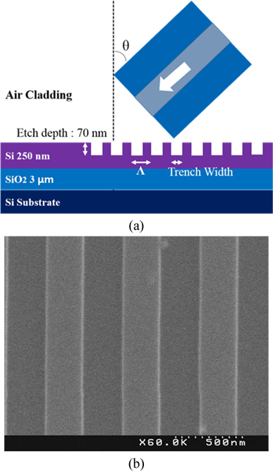
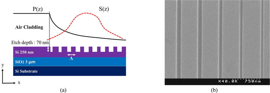
A uniform grating coupler is a simple, basic structure with a constant grating period and fill factor, as shown in Fig. 1 [2]. Its design and fabrication is relatively simple, due to its periodic structure and loose minimum pattern size. The fundamental coupling condition of a GC follows the Bragg condition [12],
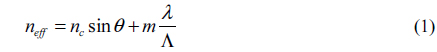
where neff is the effective index of the waveguide, nc is the refractive index of the upper cladding covering the top of the grating, θ is the coupling angle with respect to the axis normal to the grating surface, m is the order of the diffraction mode, λ is the wavelength of light, and Λ is the grating period. The portion of the etched area in the grating groove region depends on the fill factor (ff), which means the ratio of the etched width to the grating period, i.e. ff = Trench width / Period.
Numerical simulation and experimental measurement of the coupling efficiency of the GCs are performed for the configuration shown in Fig. 1. An SOI wafer with 250-nm thick silicon, 3-μm thick SiO2 buffer layer (BOX layer) on a silicon wafer, and an air top cladding is considered for our analysis. A small etch depth [13] and a tilted angle of the coupling fiber [3] are known to improve the coupling efficiency by reducing secondary back reflection. In this research the etched depth of the grooves of the GCs is fixed at 70 nm, and the coupling angle of the optical fiber with respect to the vertical axis normal to the grating surface is set to 11.5°. These fixed values of etched depth and coupling angle are used in the following numerical analysis and experimental demonstration. The finite-difference time-domain method (Lumerical’s FDTD Solutions) is used for numerical simulation. Mesh sizes of Δx = 20 nm and Δy = 10 nm are used in the numerical simulation.
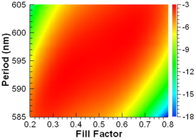
The calculated coupling efficiencies of a GC with various grating periods Λ and fill factors ff at a wavelength of 1550 nm are plotted in Fig. 2. The center of the fiber core is positioned above the groove, 5.5 μm away from the beginning of the grating coupler. From the calculated results, the maximum coupling efficiency of the GC appears to be above -2.9 dB at Λ = 592 nm and ff = 0.35. These parameters are guidelines for further optimization of the UGCs.
The calculated structures of the GC devices have been fabricated on a standard SOI (SOITECTM) wafer with a 250-nm thick silicon core layer and a 3-μm thick SiO2 BOX layer. Electron-beam (e-beam) lithography and an inductively coupled plasma-reactive ion etching (ICPRIE) process at the National Nanofab Center (www.nnfc.re.kr) have been used for the device fabrication. First, a 450-nm wide strip waveguide is connected to a 500-μm long taper, and then to a 15-μm wide platform, to form the GC on both ends. All these waveguide platforms are formed using e-beam lithography and a full dry etching of the upper silicon layer, down to the top of the lower clad BOX layer. Then, further photoresist coating, e-beam writing, and etching steps follow to pattern shallow etched trenches 70 nm deep on the GC platforms, and to form the Bragg gratings.
The characteristics of the fabricated GCs have been measured under illumination by a superluminescent diode (SLD) with an optical spectrum analyzer (OSA). The output polarization of the SLD is adjusted using a fiber-type polarization controller (PC). The input and output optical beams to and from the GCs are coupled in and out with single-mode fibers, which are placed on a fiber-mounting zig with an 11.5° tilt angle with respect to the axis normal to the surface of the GCs. The coupling efficiency is determined by measuring the maximally coupled optical beam power during fine alignments of the fibers with respect to the GCs with five-axis translation and rotation stages, monitored with a CCD camera.
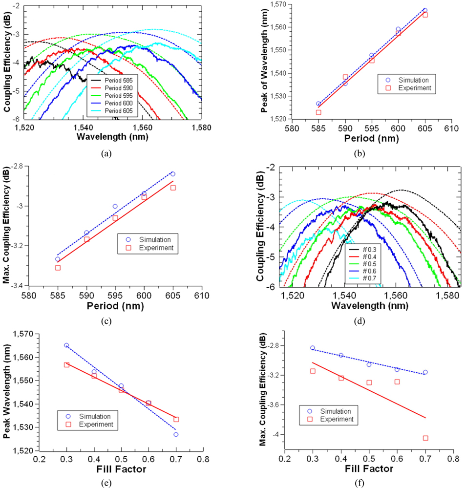
The dependence of the UGC’s coupling efficiency on the optical beam wavelength and on the grating period and fill factor is calculated by FDTD simulation, and measured by fabricating the devices experimentally. Figure 3(a) shows the simulated (dotted lines) and measured (solid lines) coupling efficiencies as functions of the wavelengths for grating periods from 585 nm to 605 nm in 5-nm increments, at a fixed value of ff = 0.5, an incident angle of 11.5°, and a constant etch depth of 70 nm. The measured results are a little lower than the simulated ones, potentially due to deviation of the fabricated devices from the calculated values of groove size and trench depth, which may be attributed to the fabrication tolerance and the side-wall roughness of grooves and waveguide. The fabrication error is analyzed to be about ±10 nm, which is smaller than the minimum pattern size of 179 nm considered in this section. Thus the low coupling efficiency measured for the fabricated UGC compared to the simulated value may be caused by differences in side-wall roughness and etch depth from the calculated design. The waveguide loss is determined from the transmittance measurement of waveguides of the same type with various lengths, and measured to be 0.28 dB/mm. The taper loss is measured to be -1.12 dB, by comparing the output of the GC with a couple of tapers to that for the non-tapered GC structure.
The relationship between peak wavelength of the UGC and grating period is shown in Fig. 3(b), the data of which are extracted from Fig. 3(a). The peak wavelength is proportional to the period, as expected from the Bragg condition in Eq. (1) and observed in Ref. [14]. The shift ratio of the peak wavelength with grating period is determined to be dλp/dΛ = 2.084 nm/nm from linear fitting of the simulated and measured data. When the grating period is changed by an amount of 20 nm, the total wavelength shift is about 40 nm which is much narrower than half of the peak wavelength in the range of λ = 1.52 - 1.58 μm inside the silicon. Figure 3(c) also shows that the maximum coupling efficiency increases with grating period, almost linearly within a period range of about 20 nm from 585 nm to 605 nm. When a light beam in the silicon core waveguide reaches the grating section, the grating patterns scatter it. It is preferred to have the scattered beams interfere constructively toward an upper coupling fiber core, and destructively downward below the waveguide. Thus the directionality of the scattered beam from the grating coupler to the coupling fiber is related to the upward constructive interference condition. The increased grating period causes a high diffracted beam intensity, just as the largely ruled grating provides a highly diffracted spectral beam. This mechanism can be understood as an optical beam having a high directivity and low angle diffraction of the input beam at a large slit. As the grating pattern size increases, the beam scatters in a smaller angle, and thus a stronger constructive fringe is possible. As long as the scattered beam profiles from the grating patterns show enhanced constructive interference at the input core end of the coupling fiber, with increasing grating period within our given wavelength range, the increased coupling efficiency is possible. The shift ratio of the maximum coupling efficiency to the grating period is determined to be dαc/dΛ = 0.021 dB/nm.
Figrue 3(d) displays the simulated (dotted lines) and measured (solid lines) coupling efficiencies as functions of wavelength for various fill factors (ff) from 0.3 to 0.7 in increments of 0.1, with a fixed grating period of 595 nm. The fill factor is varied by changing the trench width from 179 nm to 417 nm. As the fill factor changes, the peak coupling wavelength and maximum coupling efficiency vary. Figure 3(e) and (f) are extracted from Fig. 3(d). The peak wavelength and maximum coupling efficiency vary with the increase of the grating fill factor of the UGCs [14]. Variation of the fill factor changes the effective index of the grating coupler section: As the fill factor increases, the effective index of the grating coupler decreases. The peak wavelength of the grating coupler gets shorter with decreasing effective index, as expected from equation (1), and thus with increasing fill factor, as shown in Fig. 3(e). The decreased effective index of the grating coupler with increasing fill factor causes a low index modulation of the grating structure, and thus results in decreased coupling efficiency, as shown in Fig. 3(f). The shift ratios of peak wavelength to grating fill factor are determined to be dλp/dff = -9 nm/0.1 and -5.8 nm/0.1 respectively, from linear fits to the simulated and measured data, while those of the maximum coupling efficiency to grating fill factor are dαc/dff = -0.085 dB/0.1 and -0.185 dB/0.1 respectively. These characteristics of the UGCs are summarized in Table 1.
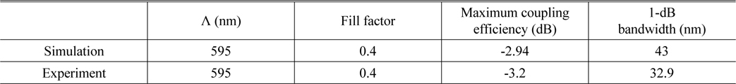
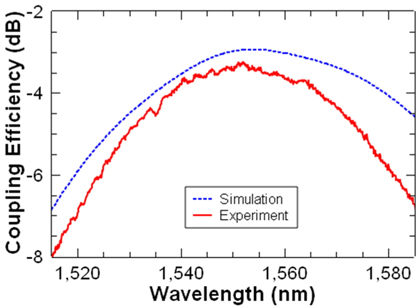
The measured maximum coupling efficiency is -3.2 dB at a wavelength of 1552 nm, with a 1-dB bandwidth of 32.9 nm when the grating period = 595 nm and ff = 0.4, compared to the calculated maximum value of -2.94 dB with a 1-dB bandwidth of 43 nm at 1553.7 nm. The simulated and measured optimum parameters and maximum coupling efficiencies of the UGCs are summarized in Table 2. Figure 4 presents the simulated and measured spectral profiles of the coupling efficiency of an UGC with the optimized parameters (Λ= 595 nm, ff = 0.4).
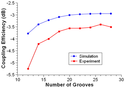
The dependence of the coupling efficiency of the UGC on the number of grooves, at a wavelength of 1550 nm, is shown in Fig. 5. The grating period and fill factor of the UGC used in Fig. 5 are the same as those used in Fig. 4. If the number of grooves is smaller than 17, the grating area is narrower than the fiber core size, which leads to a low coupling efficiency. As the number of grooves increases, the coupling efficiency increases exponentially and starts to saturate after 20 grooves, which corresponds to a grating length of 11.94 μm.
It is known that the mode mismatch between the beam profile in the fiber core and the scattered beam profile from the UGCs causes an optical coupling loss of about 1 dB [7]. As illustrated in Fig. 6(a), the internal beam power P(z) in the waveguide core starts to decrease exponentially from the start of the grating structure, as the beam propagates through it. This means that the scattered beam power profile from the surface of the grating structure has the shape of an inverted exponential decay, and does not match well the Gaussian beam profile S(z) of the single-mode fiber. Many efforts have been made to reduce this unmatched coupling problem, by modifying the spatial profile of the scattered beams from the GCs. One method to overcome the loss caused by the mode mismatch is the use of varied etch depths. Li et al. [5] used a double-etched apodized waveguide GC structure, and Tang et al. [6] used a GC structure of nonuniform grooves, with different widths and depths. However, these GC structures require either additional etching steps to have dual depths, or a sophisticated etching process to have different etching widths and depths. Another simple method is the use of a NGC with varied trench widths, which can be fabricated in conventional etching steps without forming any overlayer [3-7, 10]. This type of NGC requires a careful design to achieve an optimum scattered beam profile from the grating section, for a proper mode matching with the optical fiber. He et al. [7] demonstrated a NGC with a simple, linear fill-factor variation to reduce the mode mismatch, by fabricating the device with 248-nm DUV optical lithography. The linear variation of the fill factor offers a simple device structure for easy fabrication and optimization. In this chapter we investigate the parameter dependence of NGCs with linearly varied fill factor, and present calculated and measured coupling efficiencies of the NGCs with optimum parameters.
The formula for linear variation of the fill factor ff is considered as [7]

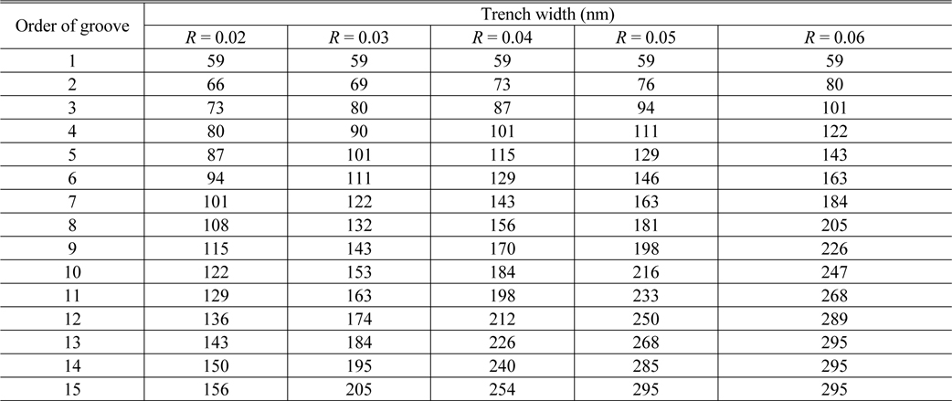
where fs is the starting fill factor of the first trench, which defines the first trench width, i.e. 1st trench width = period × fs, and the size of which is limited mostly by the lithography and etching processes. R is the rate of fill factor increment per unit length. The fill factor increases linearly with the increasing distance x from the starting point of the GC, as shown in equation (2), until it reaches the final fill factor fe, after which the fill factor becomes uniform. In our analysis we choose the grating’s parameters to be a grating period Λ of 590 nm, fs of 0.1 (corresponding to a first trench width of 59 nm (=Λ/10)), a fiber tilt angle θ of 11.5°, and fe of 0.5. The simulation conditions are the same as used in Section II, but a finer mesh is applied for more accurate calculation results. For a few trenches at the starting point below the 100-nm long grating structure, a fine mesh size of Δx = 10 nm and Δy = 10 nm is used. The coupling fiber is set at a position 8 μm away from the beginning of the GC. The trench widths calculated by equation (2) for various R values are summarized in Table 3.
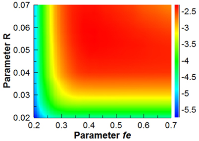
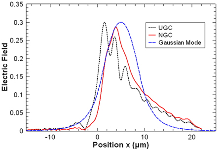
We have calculated and measured the coupling efficiencies of the NGCs for various R values and for a fe value to achieve the maximum coupling efficiency around the wavelength of 1550 nm. Fig. 7 shows a contour map of the calculated coupling efficiency as functions of R and fe. The fe value indicates the last value of the trench width change. As the fe value increases, the latter portions of the GC change into large pattern sizes. As illustrated in Fig. 7, the front portion of the GC significantly affects the coupling efficiency. Thus, the coupling efficiency changes a lot at low fe, but saturates to a constant value as fe increases above 0.4. The R value determines how fast the trench width changes, and affects the scattered beam profile from the GC. The maximum coupling efficiency is -2.305 dB at R = 0.058 and fe = 0.42. The coupling efficiency in the range of 0.04 < R < 0.07 and 0.4 < fe < 0.6 is better than -2.5 dB. As shown in Fig. 8, the scattered electric field profile from the optimized NGC is closer to the Gaussian-mode beam profile at the fiber core than that of the UGC.
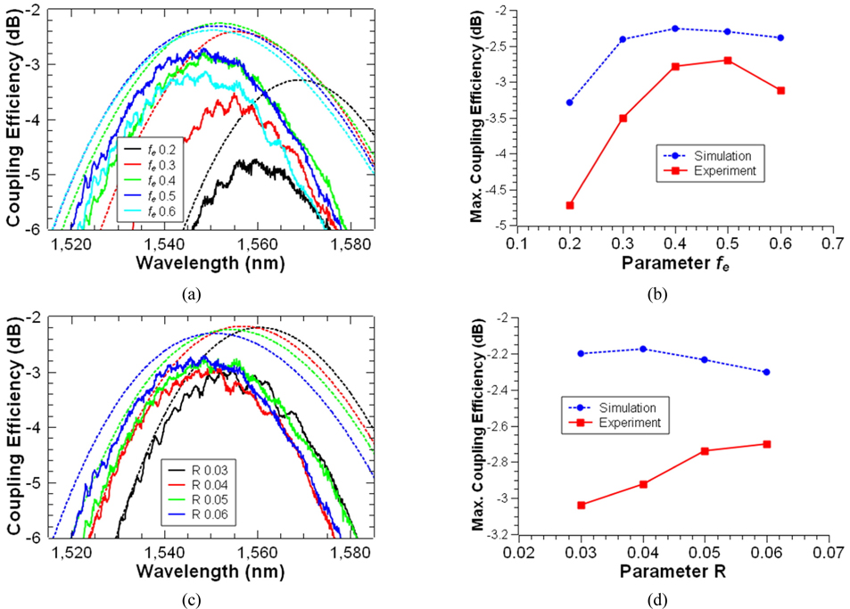
Calculated and measured coupling efficiencies for various R and fe values are shown in Fig. 9. Figure 9(a) shows the spectral profiles of the coupling efficiencies of the NGC for various fe values at R = 0.06, and Fig. 9(b) illustrates the calculated and measured maximum coupling efficiencies as functions of the fe. As discussed in the UGCs of the previous Section, the effective index of the grating coupler decreases with the increasing fill factor, and thus the peak wavelength of the grating coupler gets shortened. As expected in the simulation, the maximum coupling efficiency of the grating coupler changes significantly when fe increases within the range of low fe values, but shows little variation when fe increases above 0.4. It is confirmed that the latter patterns of the grating coupler do not affect the coupling efficiency significantly, when fe is above 0.4. The measured values are lower than the calculated ones, probably due to the fabrication tolerance, as for the UGC case discussed in Section II. The measured peak of the maximum coupling efficiency appears at fe = 0.5. Figures 9(c) and (d) present the coupling efficiencies of the NGCs when R increases from 0.03 to 0.06 for a fixed fe = 0.5. Since the trench width increases rapidly with increasing R, the effective index of the GC decreases, and thus the peak wavelength also decreases, as shown in Fig. 9(c). In Fig. 9(d), the simulation data show the tendency of the maximum coupling efficiency to a steady decline with R values above 0.04, but the measurements present a countertrend. The reason for this mismatch may be attributed to the fabrication tolerance. As shown in Table 3, the trench-width difference between two adjacent trenches is only of the order of 10 nm, which is almost the same as the fabrication error. This is an important problem for NGCs, and is why conventional grating couplers are fabricated in the UGC structure when elaborate fabrication technology is not available. A future challenge for device fabrication technology is to have better fabrication resolution and reduce fabrication error.
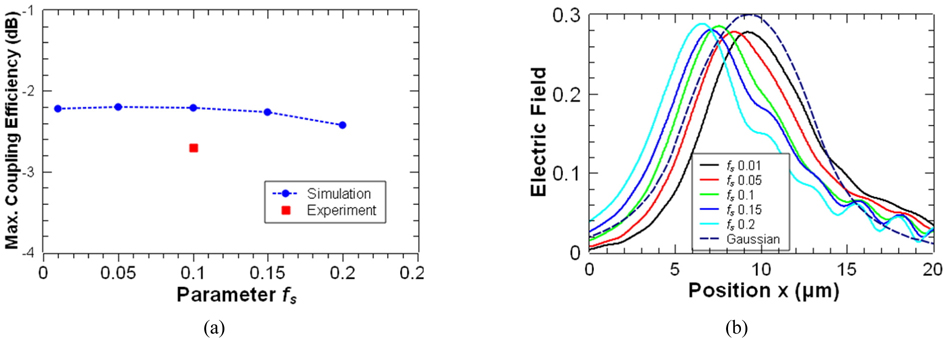
To identify the ultimate limit of coupling efficiency for the NGCs, we calculate the maximum coupling efficiency of the NGC structure and the scattered field profiles from its grating structure for various fs values. Figure 10(a) shows the calculated maximum coupling efficiency for various fs values with fixed parameters of period = 590 nm and fe = 0.5. The optimum value of the parameter R is R = 0.05 at fs = 0.01 and 0.05, R = 0.1 at fs = 0.15, and R = 0.03 at fs = 0.2. The corresponding width of the first trench for each fs value is 6, 30, 59, 89, and 118 nm. In this simulation, a fine mesh of Δx = 2 nm and Δy = 10 nm is used, for accurate calculation results. The maximum coupling efficiency is -2.2 dB when fs = 0.05, and this value is 0.02 dB larger than those when fs = 0.01 or fs = 0.1. The coupling efficiency decreases as fs increases above 0.05. Figure 10(b) shows that the overlap of the scattered beam profile from the grating structure with the Gaussian mode profile of the coupling fiber is maximum at fs = 0.05, while the mismatch between the scattered beam profile and the Gaussian mode profile increases as fs increases. A larger fs value means a wider first trench, and the wider trench induces a relatively narrower beam scattering angle. Our numerical simulation shows that the maximum overlap of the scattered beam profile with the Gaussian mode profile of the fiber occurs when fs = 0.05 (i.e. a corresponding first trench width of 30 nm). This trench width cannot be fabricated with the device processing facility available to us, due to limited fabrication tolerance. We have demonstrated experimentally a maximum coupling efficiency of -2.7 dB with fs = 0.1 (i.e. a corresponding first trench width of 59 nm), near the limitations of the fabrication processes.
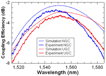
The measured maximum coupling efficiency of the fabricated NGC is -2.7 dB with R = 0.06 and fe = 0.5. Its 1-dB bandwidth is 29.9 nm, and the center wavelength is 1548.9 nm. The simulated maximum value is -2.3 dB with a 1-dB bandwidth of 37 nm at 1550 nm. The calculated and measured coupling efficiencies of the optimized UGC and NGC (fs = 0.1, R = 0.06, and fe = 0.5) are shown in Fig. 11. The peak coupling efficiency of the NGC is about 0.5 dB higher than that of the UGC. No significant difference of the measured 1-dB bandwidth is observed between the UGC and NGC.
We have investigated the optimum conditions of UGCs and NGCs for efficient coupling to single-mode fibers, in both numerical simulation and experiment. Our simulation indicates that NGCs provide better coupling efficiencies compared to UGCs, and that the peak coupling efficiency of the NGCs is possible with a starting fill factor of the first trench fs = 0.05 (i.e. a corresponding trench width of 30 nm). Within the tolerance of the device fabrication process, our measured maximum coupling efficiencies of the fabricated UGC and NGC are -3.2 dB and -2.7 dB respectively, both around the wavelength of 1550 nm, while the calculated values are -2.94 and -2.3 dB respectively. The measured 1-dB bandwidths are 32.9 nm for the UGC and 29.9 nm for the NGC, while the calculated values are 43 nm and 37 nm respectively. From our analysis we have found that further improvement of the coupling efficiency of the NGCs is possible with state-of-the-art fabrication technology of the nano-silicon waveguides, because accurate control of miniature pattern sizes on the order of 10 nm is needed.