Ever increasing demand for microwave operated applications has cultivated need for high-performance universal systems capable of working on multi-bands. This objective can be realized using Multi-Dielectrics in RF MEMS capacitive switch. In this study, we present a detailed analysis of the effect of various dielectrics on switch performance. The design consists of a capacitive switch and performance is analyzed by changing the dielectric layers beneath the switch. The results are obtained using three different dielectrics including Silicon nitride (7.6), Hafnium dioxide (25) and Titanium oxide (50). Testing of proposed switch yields high isolation (- 87.5 dB) and low insertion loss (- 0.1 dB at 50 GHz) which is substantially better than the conventional switches. The operating bandwidth of the proposed switch (DC to 95 GHz) makes it suitable for wide band microwave applications.
RF MEMS has seen an exponential growth in last decade due to its immense commercial and defense potential. These switches provide high isolation, low insertion and excellent linearity that are hard to achieve in semiconductor devices. Other key advantages include - the ability to reduce the sample size of measurands and ability to integrate sensing, analysis and response in a miniature package [1]. But this technology suffers from low switching speed, high actuation voltage, reliability issues and low power handling capabilities [2]. These switches are of two broad categories:- including the metal-to-metal contact (series) switch and shunt switch. The shunt switch is placed in shunt (perpendicular) between the T-line and ground; and depending on the applied bias voltage, it either leaves the T-line undisturbed or connects it to the ground. Therefore, the ideal shunt switch results in zero insertion loss when no bias is applied (up-state position) and infinite isolation when bias is applied (down-state position). Contact shunt switch provides excellent isolation between 10 - 120 GHz [3]. High values of dielectric materials are preferred to achieve sound isolation between 0 - 10 GHz. Conventional RF MEMS switches encompass a bridging membrane suspended over the dielectric layer that offers low insertion loss and average isolation in a single band. The MEMS shunt switch can be integrated into a Coplanar Waveguide (CPW) or in a micro-strip topology.
RF MEMS switches are applicable in the testing equipment of RF instrumentation, military tactical radio and telecom infrastructure. MEMS technology has revolutionized the field of electronics since it facilitates devices and applications that have high potential to upgrade the performance of communications systems and circuits. The realization of micro size electromechanical switches in electronics devices has led to reduction in the size thereby making them more flexible and suitable for little/light space applications.
In this study, we present a novel approach of using more than one dielectric for designing a robust low-loss MEMS switch that operates in multi-bands. Developing a switch by using different dielectric materials with a considerable difference in their dielectric constants will provide isolation at various frequencies enhancing multi-band operation. Gold (Au) has been proposed which due to its anti-stiction property achieves the constraint of operating on low voltage. The switch has been designed over a silicon substrate of thickness 100 μm with the Coplanar Waveguide (CPW) of dimensions - 55/90/55 (μm).
A typical shunt switch can be used to obtain isolation in a desired frequency band. In this paper, a switch is designed with different dielectrics to enhance isolation and switch operation in multiple bands. The switch is based on 50 Ω CPW line of 55/90/55 (μm) over a 100 μm substrate.
Gold material is used to design the CPW due to its better stiction with Silicon nitride as dielectric over the substrate [4]. Titanium oxide with relative dielectric constant of 50, Hafnium dioxide (to provide isolation between 0 - 10 Hz) with relative dielectric constant of 25, Silicon Nitride (to provide good isolation at higher frequencies) with relative dielectric constant of 7.6 has been used. Using different dielectrics will result in different values of down-state capacitance. Hence, the switch would perform in different frequency bands. The dielectric thickness has been kept as low as 0.1 μm.
Bridge membrane of thickness 1 μm has been laid over anchors of height 3 μm each. Care should be taken to optimize the thickness of the membrane to avoid breakage due to stress produced during bending. Gap height between dielectric and membrane is kept as 2.9 μm. It is necessary to optimize pull-down voltage and gap to avoid self-biasing and external vibrations on the membrane. Therefore, membranes are united with the anchor to achieve high recovery force thus aiding to recover the membrane’s position [5].
The membrane designed for the switch has the thickness of 1 μm and is made of Gold (Au) because its conductivity [0.452.106/cm] is better than Aluminium (Al) [0.377.106/cm] and better conductivity promises lesser skin depth [6]. Also, Gold possesses lower Young’s Modulus, thus, lowering the stiffness and leading to reduced pull-down voltage.
As the substrate is the base over which the switch operates, so surface needs to be flat and smooth. Uniform electrical properties and chemical resistance are other considerations during fabrication and these requirements are well satisfied by Quartz (SiO2). We used Quartz as a substrate due to this property. Quartz (SiO2) has a high melting point as compared to Silicon (Si), hence, switch designed with Quartz substrate can withstand high temperatures than the switch made on silicon substrate [7]. Quartz also provides better isolation in RF MEMS switch when compared to that of Silicon.
Hafnium dioxide (HfO2) of 0.5 μm thickness is used as a substrate dielectric. It is always preferable to use materials with high dielectric constant (K) [8]. The performance of Silicon nitride (Si3N4) (K ~ 7.6), Hafnium dioxide (HfO2) (K ~ 25) and Titanium oxide (TiO2) (K ~ 50) as switch dielectrics has been examined with the parameters of the evaluation as insertion, isolation and switch bandwidth. An attempt has been made to design the switch that can operate on multiple frequency bands.
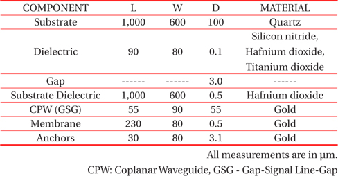
The switch has been designed using Ansoft HFSS 14 whose specifications are cited in Table 1.
[Table 1.] Hardware specifications of Switch.

Hardware specifications of Switch.
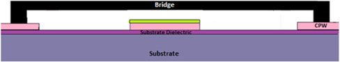
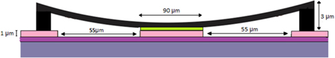
Figure 1 shows the switch structure when operated in up-state. In this case, signals pass through a transmission line with minimum loss. The switch is actuated by applying a pull-down voltage. A DC voltage is applied between the MEMS Bridge and the microwave line. This results in an electrostatic force that causes the MEMS Bridge to collapse on the dielectric layer, thereby increasing the bridge capacitance by a factor of 30 - 100 (Fig. 2). This capacitance connects the T-line to the ground and acts a short circuit at microwave frequencies, resulting in a reflective switch. When the bias voltage is removed, the MEMS switch returns to its original position due to the restoring spring forces of the bridge (Fig. 1). Down-state capacitance value increases due to the reduction in the gap leading to greater isolation. The capacitance in the up-state is kept as low as possible to maintain the high capacitive ratio. The bridge membrane has dimension of 230 × 80 μm which may be modified depending on the required switch capacitance. The length is rarely shorter than 200 μm due to the sharp increase of the actuation voltage with decreasing bridge length. The width is practically limited to 200 μm so as to result in a flat contact area between the MEMS Bridge and the T-line.
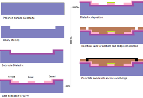
The fabrication of the proposed switch is relatively easy. The Low-stress thin-film process of development for the membrane material is the only critical step. Prerequisites for the membrane are low biaxial residual stress and a low-stress gradient in the vertical direction [9].
Figure 3 shows the complete fabrication process that is similar to the standard fabrication flow.
·To obtain semiconductor grade finish, it is mandatory to polish the surface of the substrate.
·To produce cavity, a mask is placed on the substrate. It is illuminated by UV light to transfer the pattern on the photo resist that can be further etched using an etchant.
·The Substrate dielectric layer is deposited on the etched substrate.
·Gold is evaporated to produce ground and signal line.
·A Mask is used to pattern the signal line and grounds.
For Hafnium dioxide (HfO2) - Based on the reaction mechanism, there are two techniques namely CVD (Chemical Vapor Deposition) and PVD (Physical Vapor Deposition). CVD based approaches are used in the literature [10-13]. The low cost and relative flexibility of these growth methods make them more common for depositing Hafnium dioxide.
For Titanium dioxide (TiO2) - No interfacial layer is required for effective deposition of Titanium oxide. Chemical Vapor Deposition, sol-gel deposition, and magnetron sputtering are some of the various techniques that can be employed to produce TiO2 films. Among these, the magnetron sputtering technique is considered superior as they have better adhesion to the substrate than evaporated films. DC sputtering leads to higher deposition than RF sputter [14].
For Silicon nitride (Si3N4) - Deposition is rather simpler and can be achieved using thermal oxidation in a furnace or lamped heated rapid thermal oxidation. These methods are inexpensive and exhibit good thickness uniformity.
For the fabrication of the bridge and anchor, a sacrificial layer (polyimide) is deposited. The cuts in the sacrificial layer are the sites for the deposition of metal (Au).
Gold is evaporated, and it gets deposited in the cuts of the sacrificial layer.
Figure 4 shows the proposed switch after the removal of the sacrificial layer. To remove sacrificial layer, a buffered HF solution or plasma etching [17] can be used, and the switch can be released using a critical point dryer [2].
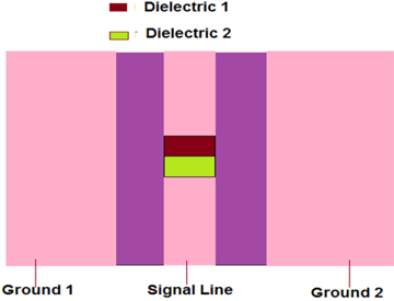
Figure 5 shows the top view of the switch and the arrangement of the dielectrics. The proposed switch will not suffer mechanical failure because the length of the switch is much greater than the deflection required for the switch [9].
The shunt switch is placed in shunt between T-line and ground and depending on the applied bias voltage; it leaves the T-line undisturbed or connects it to the ground.
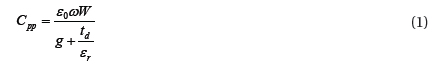
In the off-state, switch possesses up-state capacitance, which can be calculated as:

Where ‘ω’ is the width of the metal bridge, ‘g’ is the gap and ‘W’ is the width of CPW (Coplanar Waveguide), central conductor.
If the second term of denominator [td/εr] in eq. (1) is neglected due to the finite thickness of the dielectric layer, the capacitance can then be given by
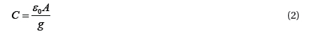
Where ‘A’ is the overlap area between the metal bridge and ‘W’ is the width of the CPW central conductor.
The dielectric constants used for evaluation of switch performance are 7.6, 25 and 50, and the dielectric layer thickness is 0.1 μm with a gap height (go) of 3 μm. So when the second term in denominator [td/εr] in eq. (1) is neglected; results in an estimation of the up-state capacitance by 6%. When the voltage is applied to membranes, the membrane snaps down onto the dielectric, resulting in the diminishing of gap. This leads to increase in down-state which can be calculated as:
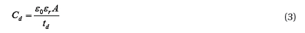
Low value of up-state capacitance and high value of down-state capacitance leads to a high capacitive ratio which further enhances RF performance of the switch.
It is required to have low value of up-state capacitance (to have minimum insertion loss) and high value of down-state capacitance (to have maximum isolation) which leads to high capacitive ratio. RF response is the function of the ratio of up-state capacitance to the down-state capacitance. Ideally capacitive ratio value is 100:1 and can be obtained by

The calculated values of up-state capacitance, down-state capacitance and capacitive ratio for different dielectrics are mentioned in table 2:
[Table 2.] Capacitive Ratio of Dielectrics.
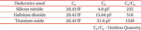
Capacitive Ratio of Dielectrics.
Table 2 clearly shows that capacitive ratio is highest for high dielectric (K) material. Thus, higher dielectric constant materials are generally employed to achieve excellent performance in RF MEMS.
The switch bandwidth is calculated from the lower and the upper operating frequency. Lower frequency (FL) is limited by the minimum isolation, whereas the upper frequency (FU) either by maximum insertion or minimum isolation. For bandwidth calculation, an acceptable maximum insertion loss of 0.3 dB and minimum isolation of 20 dB has been chosen. From Fig. 6, it is clear that switch spans around large frequency band ranging from 5 - 100 GHz with reasonable isolation below - 20 dB. Thus, the bandwidth of the switch is 95 GHz (range: DC - 95 GHz) which is much better when compared to conventional designs.
The actuation voltage (Vp) of MEMS switch with spring constant, k is given by:
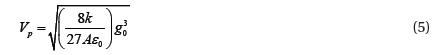
where ε0 is the permittivity of free space, go is the gap between membrane and electrode, A is an area of the electrode that comes in contact with dielectric. The value of permittivity (ε0) and spring constant (k), are fixed, thus the value of actuation voltage completely depends on the gap height between membrane and signal line. The analytical value of actuation voltage is 16.28 V.
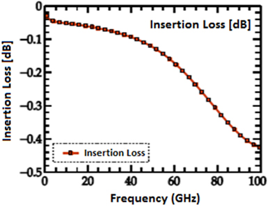
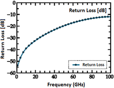
The RF Parameters for the design are extracted using S-parameters. The switch performance is observed between 5 - 100 GHz. Insertion, Isolation and Return loss are the parameters that decide the switch performance. The proposed switch exhibits excellent RF performance. Moreover, the switch operates in multiple frequencies serving as a multi-band switch. It possesses an excellent insertion of - 0.4 dB over 0 - 100 GHz. Return loss value ranging from 50 dB - 20 dB was observed over 0 - 60 GHz as seen in Fig. 7.
The performance of the switch in terms of isolation, when simulated for different combinations of dielectric is provided in Table 3.
[Table 3.] Calculated Isolation with different Dielectrics.
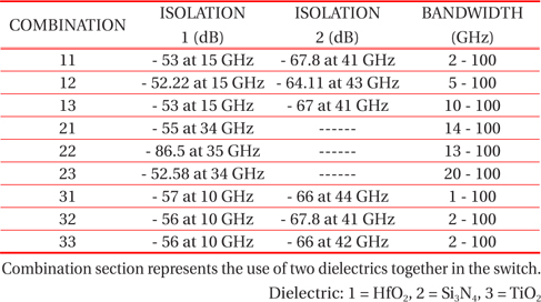
Calculated Isolation with different Dielectrics.
On examination of isolation from Table 3, maximum isolation perceived is - 86.5 dB when both are Silicon nitride (Si3N4), which is the highest value of isolation obtained by the presented switch.
Observed isolation occurs at two different points when operated with high dielectric material, thus rendering switch as a multi-band switch. Thus high dielectric material aids in switch operation at multiple frequencies. This phenomenon can be well observed in Fig. 8.
To achieve multi-band operability, we can either vary the actuation area or can change the dielectric material. Various approaches like combination of series and shunt switch that provide multi-band functionality in MEMS switch have been proposed [15]. In [16], the actuation area was varied by splitting the bridge and constructing two unsymmetrical cantilevers. But literature clearly indicates the inefficiency of the existing switches [15,16] to operate on wide bandwidth. To overcome this limitation, proposed switch uses multi-dielectric approach and achieves impressive results. Detailed comparison (refer Table 4) between conventional switch [16] and proposed switch is done on the basis of physical specifications, operable frequency range, isolation, insertion and actuation voltage. Figure 8. demonstrates the difference of isolation of both the switches. It can be easily concluded from the Figure that isolation of the proposed switch outperforms the conventional switch with the margin of 40 dB.
[Table 4.] Performance Comparison of Miniature MEMS switch.
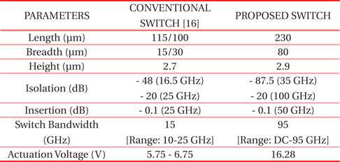
Performance Comparison of Miniature MEMS switch.
The results suggested that gap between membrane and dielectric, dielectric thickness and actuation area are not the only factors that affect RF response of switch rather the dielectric material employed also played a significant role.
In this study, three dielectrics - Silicon nitride (Si3N4), Hafnium dioxide (HfO2) and Titanium oxide (TiO2) has been used in different combinations and some of the main point of inference is:
· High dielectric constant provides excellent isolation at lower frequencies.
· The dielectric layer that is towards the input port asserts the maximum effect on the RF response of the concerned switch because the first switch blocks the maximum signal.
· Low K (dielectric constant) dielectric materials provide isolation in specific band while high K dielectric gives isolation at multiple frequencies thus making it work on multi-bands as observed in Table 3. [18-20] compares the measured results with simulated results and consequently shows that there is a little deviation in actual performance and simulated results of the switch. So the simulated results presented in the paper would be similar to the actual performance.
The earlier proposed methods for obtaining multi-band operation were based on combination of series and shunt switches [15] or changing the actuation area [16]. Method proposed in this paper is novel as it uses the difference in dielectric constant of dielectrics to achieve multi-band operation.
The proposed switch utilizes a novel approach to switch design that lays focus on the role of dielectric in enhancing the RF performance and operability of the switch. From the numerical calculations and simulations, it is clear that the suggested switch exhibits excellent isolation and insertion loss. It is also evident that high K dielectric promotes multi-band operations. Due to its excellent RF response and multi-band functionality, the switch is applicable when low loss, low power or multi-band operation is a primary concern such as in Wireless Communications and Space systems.


![Isolation of Conventional [16] vs Proposed Switch.](http://oak.go.kr/repository/journal/20678/E1TEAO_2016_v17n2_86_f008.jpg)