Indium phosphide (InP) has been a promising material in the field of electronic devices such as laser diodes, photo-detectors, solar cells, high electron mobility transistors (HEMTs), high speed metal-insulator-semiconductor field effect transistors (MISFETs), microwave sources and amplifiers due to its direct band gap, good temperature stability, high frequency response and high electron saturation velocity (2.5 × 107 cm/s) [1-5]. In order to realize such devices the electrical properties of metal-semiconductor (MS) interface must be thoroughly understood. The progress in InP devices has been limited by low Schottky barrier height, poor stability and large reverse leakage current [6,7]. Therefore, there has been strong attention in developing thermally-stable rectifying contacts to InP with high barrier height and low leakage current [8,9].
The electrical and structural properties of the Schottky contacts to undoped (unintentionally n-type doped) and intentionally n-type InP have been investigated by several research groups. Assuming that Fermi-level pinning is caused by a high density of surface states, passivation technology has been employed to reduce the density of surface states [6,10,11]. For example, Jeng et al. reported the barrier height as high as 0.95 eV in Ag/n-InP (S-doped InP with a carrier concentration of 5 × 1017 cm-3) Schottky diode using phosphorous sulfide/ammonia sulfide [P2S5/(NH4)2Sx] solution [10]. Modulation of the effective barrier height has been attempted by inserting an insulator or organic layer between the metal and the semiconductor layers [12,13]. For example, Soylu et al. investigated the effects of thermal annealing on Au/Pyronine-B/n-InP (S-doped InP with a carrier concentration of 1.2 × 1016 cm-3) Schottky structures, and showed that the diode parameters depended on the annealing temperature [13]. The effect of thermal annealing on the electrical properties of InP Schottky junction has also been investigated; Reddy et al. determined the effects of rapid thermal annealing on the electrical and structural properties of Pd/Au Schottky contacts to n-InP (undoped InP with a carrier concentration of 4.5 × 1015 cm-3) and reported that the formation of indium phases at the interface increasing Schottky barrier height at 400℃ [14]. Janardhanam et al. fabricated Mo/n-InP (undoped InP with a carrier concentration of 5 × 1015 cm-3) Schottky diode and investigated the electrical, structural and surface morphological properties as a function of annealing temperature. The decrease in barrier height after annealing at 500℃ was reported to be due to the formation of phosphide phases at the interface [15].
The dominant process that determines the electron transport in Schottky junction when a bias voltage is applied to the junction can be understood by considering various transport models. In addition, the analysis of temperature dependent current-voltage (I-V) characteristics is a method to investigate the physical mechanisms associated with the reverse-bias leakage current in the material. Miller et al. presented temperature-dependent I-V measurements of Schottky diodes fabricated on GaN grown by molecular beam epitaxy, [16] suggesting two dominant leakage current mechanisms [16]. Ueda et al. investigated I-V characteristics of Cu/diamond Schottky diodes at high-temperature and high-voltage characteristics and found the dominant transport mechanisms under reverse-bias condition [17]. Oxygen plasma treatment known as an effective, economic and environmentally safe method is widely used during the device fabrication process to clean the semiconductor surface and to prepare for further processing. Through such cleaning processes, residual organics, metallic contaminants and native oxides from the semiconductor surface should be removed completely during the fabrication. In this respect, investigation of the reverse-bias leakage current for oxygen plasma treated InP is meaningful to improve the device performance. Here, we explore comparatively the current transport mechanism of Cu/n-InP Schottky contacts under reverse-bias conditions with and without oxygen plasma treatment.
As a starting material, single side polished undoped (unintentionally n-type doped) InP (100) wafer (thickness: 350 μm), having a carrier concentration of ~1 × 1016 cm-3 was used. The wafer was first cut into small pieces and some of these pieces were subjected to oxygen plasma treatment on the polished side. Oxygen plasma was produced with a plasma power of 250 W at the atmospheric pressure with an oxygen flow rate of 40 sccm and an Ar flow rate of 8 sccm. After solvent cleaning, Cu Schottky contacts with thicknesses of 100 nm were deposited by using radio-frequency (RF) magnetron sputtering through a shadow mask onto the polished side for all the samples. For ohmic contacts, 150 nm thick Al metal was deposited over the entire back surface of the samples. Current-voltage (I-V) measurements were carried out in the temperature range of 100-300 K with a Keithley 4200 SCS and a cryogenic probe station (Janis ST-500). X-ray photoelectron spectroscopy (XPS) measurements were carried out using a monochromatic Mg Kα x-ray source to observe the formation mechanism of Cu/n-InP contact.
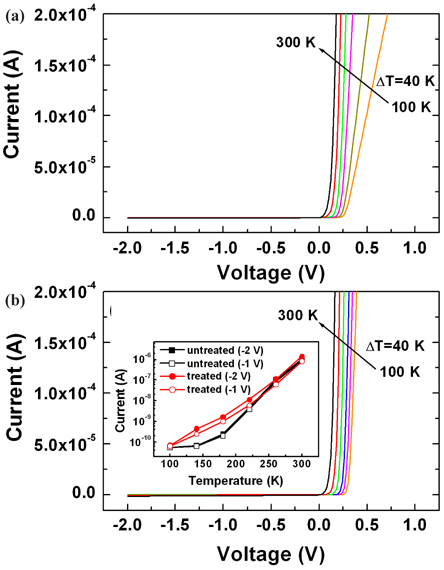
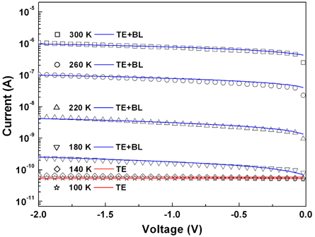
Figure 1 shows the typical linear I-V characteristics measured in temperatures of 100 K - 300 K, showing rectifying characteristics. With increasing temperature, the forward bias current values also increased for both samples. As shown in the inset of Fig. 1(b), the reverse-bias current values are similar at 100 K, 260 K, and 300 K, but these are higher for plasma treated sample at other temperatures (140 K, 180 K, and 220 K). Different transport mechanisms are indicated at intermediate temperatures.
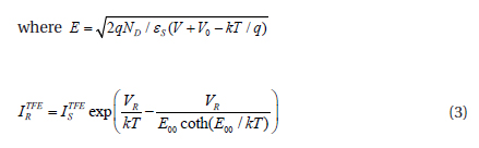
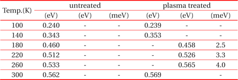
The reverse current, IR were analyzed by using various models such as TE [18], TE combined with barrier lowering (BL) [18], TFE [19], which are expressed by following equations
and
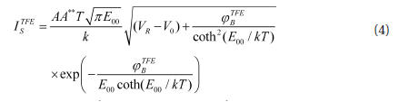
where VR is the reverse bias, A** is the Richardson constant, V0 = kT / q ln(Nc / Nd) is the potential difference between conduction band and Fermi level, E00 = (qħ / 2)( Nd/meεS)1/2 is the characteristic energy related to the tunneling probability, and and are the barrier heights for TE and TFE models, respectively. Fitting to experimental reverse-bias I-V data with theoretical I-V curves was carried out for each sample considering , E00 and as fitting parameters. Figure 2 shows comparison between the experimental and the fitted I-V curves for untreated sample. At low temperatures (100 K and 140 K), the experimental data fitted well with the TE model. The fitting values of barrier height were 0.240 eV and 0.343 eV at 100 K and 140 K, respectively. With further increase in temperature, the experimental data were explained by TE combined with a barrier lowering model. The fitting values of barrier height were 0.460 eV, 0.512 eV, 0.533 eV, and 0.562 eV at 180 K, 220 K, 260 K, and 300 K, respectively.
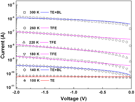
Figure 3 shows comparison between the experimental and the fitted I-V curves for plasma treated sample. At 100 K, the experimental data were fitted well by TE model. The fitting value of barrier height was 0.239 eV. At 140 K, the experimental data were fitted well with TE combined with the barrier lowering model with the fitting value of barrier height as 0.353 eV. With further temperature increase, the experimental data were explained by a TFE model instead of TE combined with a barrier lowering model. The fitting values of E00 were calculated to be 2.5 meV, 3.3 meV, and 4.0 meV at 180 K, 220 K, and 260 K, respectively. These values correspond to the apparent carrier concentration of 1.4 × 1016 cm-3, 2.5 × 1016 cm-3 and 3.7 × 1016 cm-3 at 180 K, 220 K and 260 K, respectively. In addition, these values are larger than the values of 5.0 × 1015 cm-3 ~ 1.0 × 1016 cm-3 determined from capacitance-voltage (C-V) measurements. Here, C-V data for the untreated and plasma treated samples were measured at 300 K using a Keithley 4200 SCS. Because interface states cannot follow an AC signal at sufficiently high frequencies (f ≥ 1 MHz) [20], characterization took place at 1 MHz to eliminate the contribution of these states. The carrier concentrations were extracted from the slopes of plots of A2/C2 as a function of reverse bias VR, where A is the diode area. The interface states near the surface were generated for plasma treated sample, which enhanced the tunneling probability and thus were explained by TFE model. At 300 K, the experimental data were fitted well by TE combined with barrier lowering model with the fitting value of barrier height as 0.569 eV. Considering that the current transport mechanisms were explained by TE combined with barrier lowering model at low and high temperatures and by TFE model at intermediate temperatures, the activation of interface states generated by oxygen plasma might be dependent on the temperature.
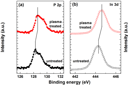
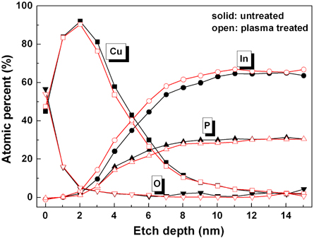
In order to investigate the contact formation mechanisms in more detail, XPS measurements were performed after depositing 10 nm thick Cu metal layers on both untreated and plasma treated InP samples. As shown in Figure 4, the peak positions of P 2p and In 3d core levels shifted to higher binding energy after oxygen plasma treatment, which indicates the surface Fermi energy movement toward the conduction band edge, resulting in a decrease in the upward surface band bending. The decreased surface band bending could lead to decreased barrier height [21]. The average Schottky barrier height from I-V measurements at room temperature for 8~10 Schottky diodes were found to be 0.469 (± 0.003) eV and 0.482 (± 0.010) eV, respectively, for untreated and plasma treated samples. Although, the XPS spectra indicated that the barrier height would decrease after plasma treatment, the results from I-V indicated the effect of oxygen plasma treatment on the barrier height is negligible.
Further information on the interfacial reaction between Cu metal layer and n-InP film was obtained from the XPS depth profiles as shown in Fig. 5. The atomic percents of O atoms present on the InP surface are similar, implying that O atoms after plasma treatment did not stay near the InP surface. Compared to untreated sample, the atomic percents of In atoms are higher and those of Cu and P atoms are lower for plasma treated sample. Both samples show that In and P atoms out-diffused into Cu metal layer, resulting in the formation of Cu-In and Cu-P interfacial phases at the interface. Figure 5 also shows that the relative P/In ratio became smaller after plasma treatment, suggesting the presence of phosphorous vacancies.
Using deep level transient spectroscopy (DLTS) measurements, Ahaitouf et al. observed the distribution of interface states with the peak at ~ 220 K with the activation energy lower than 0.2 eV [22]. Based on these results, the origin of interface states was attributed to phosphorus vacancies (VP) or indium vacancies (VIn). This trap was also attributed to interface states due to phosphorus vacancies occupied by oxygen after surface treatment [22,23]. Meanwhile, Janardhanam et al. observed the deep trap with the peak at ~ 220 K (activation energy of 0.18 eV) in Pd/n-InP Schottky diodes after annealing at 400℃ and also associated the peak with VInVP divacancy defects [24]. Using a positron-lifetime study, Shan et al. found that a large amount of VP vacancies form after PP atoms migrate to interstitial sites and then VP vacancies which are in the vicinity of indium vacancies could combine to form VInVP divacancies. [25]. Although the analysis on XPS results in this work showed that P/In atomic ratio decreased after oxygen plasma treatment, we cannot rule out the possibility that both VIn and VP might be generated after oxygen plasma treatment. Then, the interface states generated from oxygen plasma treatment could be associated to the VInVP divacancies, and these defects may contribute to the total current transport at intermediate temperatures (180 K ~ 260 K). However, further research should be performed to clarify the exact origin.
Using current-voltage (I-V) measurements, the current transport mechanisms of Cu Schottky contacts to oxygen plasma treated n-InP under reverse-bias condition were investigated comparatively. The suitable current transport models for untreated sample has changed from thermionic emission (TE) to TE combined with barrier lowering with increasing the temperature. For plasma treated samples, the experimental data were explained by TE and TE combined with barrier lowering models, respectively, at 100 K and 140 K. At intermediate temperatures, the current transport was explained by thermionic field emission (TFE) model. At 300 K, TE combined with barrier lowering model fitted well with the experimental I-V data. Probably VP involved defects (VInVP divacancies) may contribute to the total current transport at intermediate temperatures.