V2O5/Mn3O4/Nb2O5 codoped zinc oxide varistor ceramics were sintered at a temperature range as low as 875~950℃. The voltage clamping characteristics of V2O5/Mn3O4/Nb2O5 codoped zinc oxide varistor ceramics were investigated at a pulse current range of 1~50 A. The sintering temperature had a significant effect on clamp voltage ratio, which exhibits surge protection capabilities. The varistor ceramics sintered at 875℃ exhibited the best clamping characteristics, in which the clamp voltage ratio was 2.69 at a pulse current of 50 A. The varistor ceramics sintered at 900℃ exhibited the highest electrical stability, where = 3,824 V/cm (initial 3,909 V/cm), and E1 mA/cm2 = 27 (initial 39) after application of a pulse current of 100 A.
Surge is transient, such as lightning, high energy switching and high sparkover, electrostatic discharge (ESD), and electro-magnetic discharge. The generation of surge is very irregular and inside or outside facility. However, 60~80% of surges are created within a facility. In reality, high-tech products around us lie in vulnerable situations from lightning and various surges. This is attributed to a fatal weak point in which the semiconductor devices of high-tech products malfunction or are destroyed under transient overvoltage. Therefore, high-tech systems without a surge protection device (SPD) are vulnerable to damage.
The varistor is an electronic component composed of polycrystalline semiconductors, which exhibits symmetric nonohmic characteristics like a back-to-back Zener diode [1]. Typical ZnO varistor is made by sintering ZnO powder added with non-ohmic forming oxides and various subordinate oxides. The distinctive microstructure of ZnO ceramics, which composed of a lot of unit structures such as grain-grain boundary-grain, yields good non-ohmic properties and a high absorption capability for transient overvoltage. Thus, ZnO varistors have been widely used to protect various semiconductor devices, electronic circuits, and electric power systems from surges [2,3].
Commercial multilayered chip varistor ceramics should be cofired at a relatively high temperature (above 1,000℃) with an expensive refractory Pd or Pt as an inner-electrode in order to have a desirable sinterability, but new ZnO-V2O5-based ceramics can be co-sintered together with a pure Ag as an inner-electrode at a low sintering temperature of approximately 900℃ [4,5]. However, previous studies on ZnO-V2O5-based ceramics are very deficient in many points. Moreover, MnO2 doping has been investigated in many studies because MnO2 induces better non-ohmic properties than Mn3O4 [8,9,11,13,14], but since the cost of MnO2 is higher than that of Mn3O4, V2O5-doped ZnO varistors modified with Mn3O4 are being studied [10,12]. At present, there are very few published reports on the clamping characteristics and pulse aging behavior of ZnO-V2O5-Mn3O4-based varistors [15] relative to those on ZnO-V2O5-MnO2-based varistors [13,14]. In this study, the effect of sintering temperature on clamping characteristics and pulse aging behaviors of V2O5/Mn3O4/Nb2O5 codoped varistors was investigated, and some new results were obtained.
Reagent-grade raw materials were used in the following proportion: 98.95 mol% ZnO, 0.5 mol% V2O5, 0.5 mol% Mn3O4, and 0.05% mol% Nb2O5. After milling, the dried powders were pressed into disk-shaped pellets of 10 mm in diameter and 1.5 mm in thickness at a pressure of 100 MPa. The pellets were set on the MgO plate into alumina sagger, sintered at four temperatures (875, 900, 925, and 950℃) in air for 3 h, and furnace-cooled to room temperature. The sintered samples were lapped and polished. The final samples were about 8 mm in diameter and 1.0 mm in thickness. Silver paste was coated on both faces of the samples, and the silver electrodes were formed at 5 mm in diameter by heating at 550℃ for 10 min. Finally, after the lead wire was soldered to both electrodes, the samples were packaged by dipping them into a thermoplastic resin powder.
2.2 Microstructure measurement
The surface microstructure was measured using a scanning electron microscope (FESEM, Quanta 200, FEI, Brno, Czech). The average grain size (d) was determined by the lineal intercept method, given by d = 1.56 L/MN, where L is the random line length on the micrograph, M is the magnification of the micrograph, and N is the number of the grain boundaries intercepted by the lines [15]. The densities (ρ) of the sintered pellets were measured using a density determination kit (238490) attached to a balance (AG 245, Mettler Toledo International Inc., Greifensee, Switzerland).
The electric field-current density (E-J) characteristics were measured using a V-I source (Keithley 237, Keithley Instruments Inc., Cleveland, OH, USA). The breakdown field (E1 mA/cm2) was measured at 1.0 mA/cm2 and the leakage current density (JL) was measured at 0.8 E1 mA/cm2. In addition, the non-ohmic coefficient (α) was defined by the empirical law, J = C·Eα , where J is the current density, E is the applied electric field, and C is a constant. α was determined in the current density range of 1.0 mA/cm2 to 10 mA/cm2 , where α = 1/(logE2-logE1), and E1 and E2 are the electric fields corresponding to 1.0 mA/cm2 and 10 mA/cm2 , respectively
2.4 Pulse current characteristic measurement
The clamping voltage (Vc) was measured at a pulse current (Ip) of 1, 5, 10, 25, 50, and 100 A using a surge generator (Tae-yang Engineering, Busan, Korea) and an oscilloscope (TeK 3020B, Beaverton, Oregon, USA). The pulse current waveform had a width of 20 μs and a rise time of 8 μs. The clamp voltage ratio (K = Vc/V1 mA) is defined by the ratio of clamping voltage to breakdown voltage. The breakdown voltage (V1 mA) was measured at a current of 1.0 mA DC. The pulse aging test was performed at a multi-pulse current of 100 A (continuously 3 times for each pulse current) using a surge generator. After application of a pulse current, the V-I characteristics were measured at room temperature.
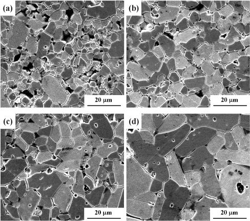
Figure 1 shows the SEM micrographs of the samples for different sintering temperatures. The average grain size (d) increased in the order of 5.9, 6.9, 9.3, and 14.3 μm with an increase in the sintering temperature. The increase in d is attributed to the in crease in surface energy with increasing sintering temperature as a deriving force for grain growth. The densities of sintered pellets decreased in the order of 5.54, 5.50, 5.46, and 5.40 g/cm3 (compare with pure ZnO, TD = 5.78 g/cm3 ) with increases in sintering temperature. This may be related to the volatility of V2O5 with low melting point (690℃) or its minor phases (VO2 and ZnV2O4) [7].
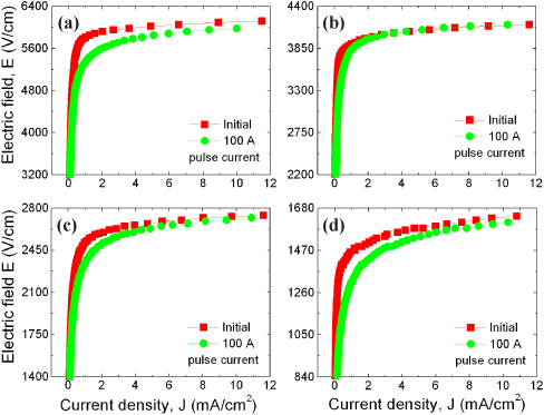
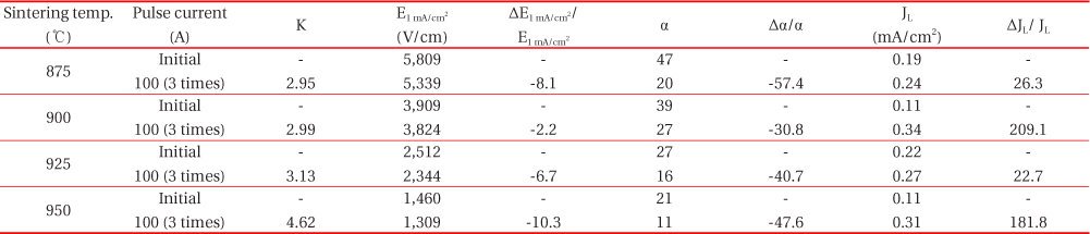
The E-J characteristics of the samples for different sintering temperatures are designated as initial in Fig. 2. The non-ohmicity of E-J curves is obvious from before and after breakdown voltage: high resistance region and low resistance region. The initial E-J characteristic parameters are summarized in Table 1. The breakdown field (E1 mA/cm2) decreased significantly from 5,809 to 1,460 V/cm with increasing sintering temperature. This is attributed to the decrease in the number of grain boundaries due to the increase in average grain size. The non-ohmic coefficient (α) decreased from 47 to 21 with increasing sintering temperature. It is noted that the samples sintered at 875 and 900℃ exhibited a high non-ohmic coefficient despite quaternary ceramics [15]. The behavior of (α) is deeply related to potential barrier height coming from donor density and density of interface states. As a result, it can be seen that the sintering temperature has a marked effect on the E-J characteristics by the tendency of change of E-J curves with increasing sintering temperature.
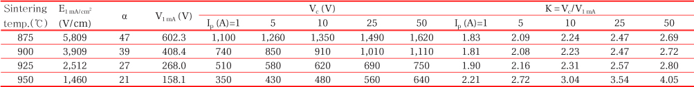
Breakdown field (E1 mA/cm2), non-ohmic coefficient (α), breakdown voltage (V1 mA), clamping voltage (Vc), and clamp voltage ratio (K) of the samples sintered at different temperatures.
The clamping voltages (Vc) corresponding to pulse currents of 1~50 A for the samples sintered at different temperatures are summarized in Table 1. Vc is defined as the voltage drop between electrodes of the sample when the specified pulse current flows through the sample. Vc is different from breakdown voltage, and is an important feature of a transient suppressor. A lower K value leads to better varistors. The K value is the clamping capability, describing the ability of the varistors to clamp the surge in the vicinity of breakdown voltage. In the pulse current range of 1~50 A, the K value generally increased with increasing sintering temperature. In general, a higher α value leads to a lower K value. For this reason, the sample sintered at 875℃ exhibited the best clamping characteristics, with K = 2.69 at pulse current 50 A. The sample sintered at 875 ~ 925℃ exhibited much better clamping characteristics when compared with ZnO-V2O5-MnO2-based varistors [13,14] and ZnO-V2O5-Mn3O4-based varistors [15]. On the other hand, the sample sintered at 950℃ exhibited a K value as high as 2.21, even at a pulse current of 1 A, and the K value greatly increased to 4.05 at a pulse current of 50 A. The non-ohmicity of this sample is not so bad when considering the non-ohmic coefficient of 21. Nevertheless, the clamping characteristics are not good. In the light of this result, it seems that this sample exhibits an unstable potential barrier at grain boundaries. As a result, it can be seen that the sintering temperature has a noticeable effect on clamping characteristics.
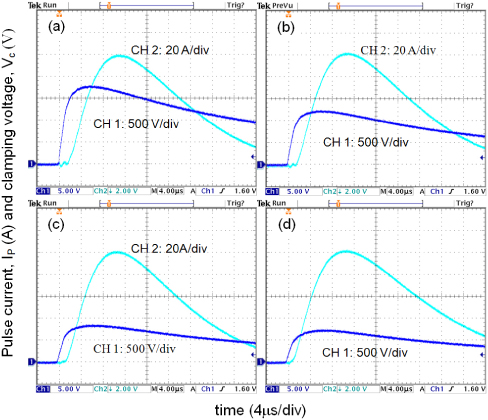
Figure 3 shows clamping voltage (Vc) characteristics corresponding to the higher pulse current (Ip) of 100 A (20 A/div) in order to investigate pulse aging behavior for the samples sintered at different temperatures. The clamping voltage increased based on increases in the electric field with increasing sintering temperature. The sample sintered at 875℃ exhibited the lowest K value (2.95) at a pulse current of 100 A.
The E-J characteristics after application of a higher pulse current of 100 A with initial E-J characteristics for different sintering temperatures are indicated in Fig. 2. The samples exhibited a noticeable difference in the variations of E-J characteristics after application of a pulse current in accordance with sintering temperature. The sample sintered at 875℃ exhibited a relatively large variation in the knee region and breakdown region after the application of a pulse current of 100 A. The sample sintered at 925℃ exhibited a similar tendency as the sample sintered at 875℃. The sample sintered at 950℃ exhibited the largest variation in E-J characteristics after the application of a pulse current of 100 A. On the other hand, the sample sintered at 900℃ exhibited relatively little variation in the knee region after the application of a pulse current of 100 A.
The variations in breakdown field (ΔE1 mA/cm2/E1 mA/cm2), nonohmic coefficient (Δα/α), and leakage current density (ΔJL/JL) after application of a pulse stress for different sintering temperatures are summarized in Table 2. The values for ΔE1 mA/cm2/E1 mA/cm2 of samples sintered at 875 ~ 925℃ were within 10% of each other after application of a pulse current of 100 A. Among the samples, the sample sintered at 900℃ exhibited the highest stability, with −2.2% in ΔE1 mA/cm2/E1 mA/cm2 after application of a pulse current of 100 A. In contrast, the sample sintered at 950℃ exhibited the lowest stability for E1 mA/cm2 characteristics with variation rates above 10% in ΔE1 mA/cm2/E1 mA/cm2 after application of a pulse current of 100 A.
Variation rates of breakdown field (ΔE1 mA/cm2/E1 mA/cm2), non-ohmic coefficient (Δα/α), and leakage current density (ΔJL/JL) before and after application of a pulse current for the samples sintered at different temperatures.
On the other hand, the α characteristics of all samples exhibited a large variation above 30%, unlike E-J characteristics, after application of a pulse current of 100 A. However, the sample sintered at 900℃ maintained relatively high non-ohmic properties, exhibiting an α value of 27 after application of a pulse current of 100 A. The samples sintered at 875 and 925℃ exhibited low variation rates in JL characteristics after application of a pulse current of 100 A, compared with other samples. It is unusual that the sample sintered at 900℃ exhibited the largest variation in JL despite having the smallest variation in E1 mA/cm2 and α. The reason for this result is unclear at present. As a result, it can be seen that pulse aging behavior is significantly affected by sintering temperature.
The effect of sintering temperature on claming characteristics and pulse aging behavior of V2O5/Mn3O4/Nb2O5 codoped zinc oxide varistor ceramics was investigated. The sintering temperature has a noticeable effect on clamp ratio, which exhibits surge protection capabilities. The varistor ceramics sintered at 875℃ exhibited the best clamping characteristics by exhibiting the lowest clamp voltage ratio at a pulse current of 100 A. The varistor ceramics sintered at 900℃ exhibited the highest electrical stability after application of a pulse current of 100 A. The sintering temperature is optimized at 875 ~ 900℃ based on nonohmicity, clamping characteristics, and stability. In conclusion, experimental results showed that V2O5/Mn3O4/Nb2O5 codoped zinc oxide varistors have great potential as multilayered chip varistors, when considering the material cost, as well as clamping and pulse aging characteristics.