We present a novel schematic using a 3-dB coupler to transmit radiofrequency (RF) power to two receivers selectively. Whereas previous multiple receiver supporting schemes used hardware-switched methods, our scheme uses a soft power-allocating method, which has the advantage of variable power allocation in real time to each receiver. Using our scheme, we can split the charging area and focus the RF power on the targeted areas. We present our soft power-allocating method in three main points. First, we propose a new power distribution hardware structure using a FPGA (field-programmable gate array) and a 3-dB coupler. It can reconfigure the transmitting power to two receivers selectively using accurate FPGA-controlled signals with the aid of software. Second, we propose a power control method in our platform. We can variably control the total power of transmitter using the DC bias of the drain input of the amplifier. Third, we provide the possibility of expansion in multiple systems by extending these two wireless power transfer systems. We believe that this method is a new approach to controlling power amplifier output softly to support multiple receivers.
Wireless power transfer (WPT) is revolutionizing the mode of electricity transmission to enable the reliable and efficient wireless charging of electronic devices. Such a transmission is especially useful in cases where interconnecting wires are hazardous or inconvenient, such as wireless sensors, for the lifespan of civil infrastructures [1]. Since a commercial wireless charging system should permit the charging of many different devices, it is important to implement an optimum system that can support multiple receivers.
If multiple devices are to be charged simultaneously on the same system, the transmitting coil must be large enough to accommodate them. However, large transmitting coils require more turns to achieve an even field distribution, which raise the coil inductance. As the inductance of the transmitting coil increases, the series capacitor in the network needs to be smaller. The class-E amplifier becomes increasingly sensitive to small variations in the component values. To circumvent this problem, the inductance could be decreased using two or more transmitting coils in parallel [2]. Recently, the horizontal (x-y plane) freedom of positioning for multiple devices has been actively conducted in the WPC’s
In this paper, we propose a novel schematic using a 3-dB coupler to transmit radiofrequency (RF) power to two receivers selectively. Whereas previous multiple receiver supporting schemes used the hardware-switched method, our scheme uses the soft power-allocating method, which has the advantage of variable power allocation in real time to each receiver. Using our scheme, we can split the charging area and focus the RF power on the targeted areas. Since the mechanism to detect the location of the receiving coil is a topic for future research, it will not be discussed in this paper. We believe that this method offers a new approach to controlling power amplifier output softly to support multiple receivers.
In this paper, we present a soft power-allocating approach using three main methods. First, we propose a new power distribution hardware structure using a FPGA (field-programmable gate array) and a 3-dB coupler. This structure can reconfigure the transmitting power to two receivers selectively using accurate FPGA-controlled signals with the aid of software. Second, we propose a power control method in our platform. We can variably control the total power of the transmitter using a DC bias of the drain input of the amplifier. Third, we provide the possibility of expansion in multiple systems by extending these two WPT systems.
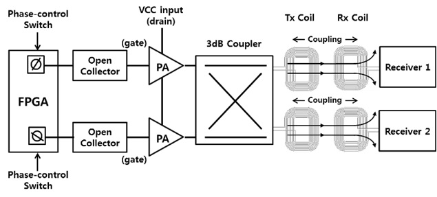
Fig. 1 shows our proposed architecture for the WPT, which is a simple structure of a multiport amplifier (MPA) with 2-by-2 amplifiers as input and output ports. The MPA is a multi-input and multi-output amplifier in which it is possible to connect the input and output ports using a Butler matrix. In the past, the MPA technique was mainly used in the development of satellite payloads [5–7]. We can extend our system using the MPA to multiple systems for future work.
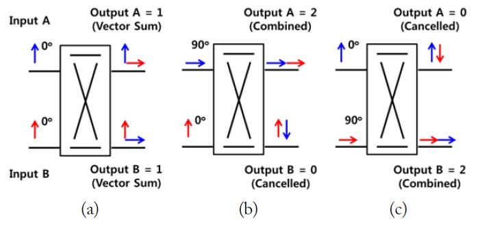
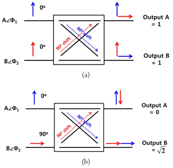
The proposed WPT architecture is composed of a phase shifter controlled by FPGA, two open collectors, two class-E power amplifiers, a four-port power combiner (i.e., 3 dB coupler), and two pairs of Tx/Rx coils. The open collector is used to boost the output voltage to 5 V to drive the switching transistor of the class-E power amplifier. Depending on the phase control of the FPGA, the power ratio of the outputs at the two transmitting coils becomes 1:1, 2:0, and 0:2, respectively, as shown in Fig. 2.
Fig. 2 shows the basic concept of the output power
The pulse source is used to adjust the magnitude and phase of the voltage, and is required to control the operation of both power amplifiers. We use the FPGA chip of the Xilinx to control the correct frequency and phase. The driving voltage of the switching transistor of the class-E power amplifier is not enough because the FPGA has a maximum output of 3.6 V. A voltage of 5 V is required to switch the transistor in our system, which uses a VRF151 transistor with a threshold voltage of 3 V. An open collector is used to boost the output voltage to 5 V to drive the switching transistor of the class-E power amplifier. We also use a toggle switch to control the phase lead or lag of the two power amplifiers.
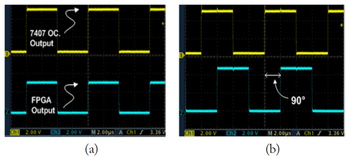
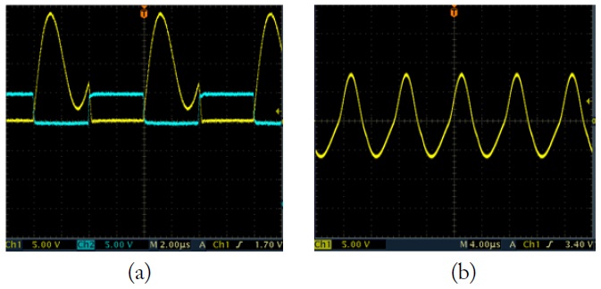
Fig. 3 shows the phase diagram of the two FPGA pulse sources. The output voltage of the FPGA is boosted to 5 V at the open collector (7407) shown in Fig. 3(a). Fig. 3(b) shows the 90° phase lag of the reference input source shown in Fig. 3(a).
3. Switching Mode Power Amplif ier Design
In the WPT system, a power amplifier with a high RF power conversion efficiency is needed. Thus, we select a class-E power amplifier as the switching mode power amplifier [8].
Fig. 4 shows the measured results of the amplifier output, which satisfies the zero voltage switching (ZVS) and the zero voltage derivative switching (ZVDS) condition in Fig. 4(a). It also shows the desired sine wave of 125 kHz with a power amplifier output in Fig. 4(b).
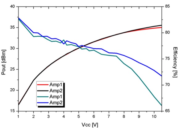
The power and efficiency of the two power amplifiers are shown in Table 1. As we expect, the two power amplifiers have a similar output power (
[Table 1.] Power and efficiency of the two power amplifiers (PAs)
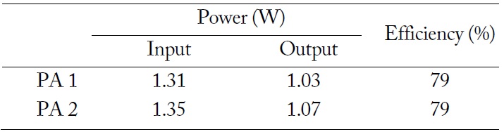
Power and efficiency of the two power amplifiers (PAs)
Fig. 5 shows the
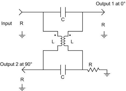
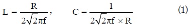
Generally, a 3 dB coupler at the high frequency band is implemented using λ/4 transmission lines, such as a hybrid coupler or Lange coupler. However, we cannot use these structures with the length of the wavelength because our system operates at a frequency band of 100–205 kHz. Therefore, we adopt a lumped quadrature coupler shown in Fig. 6, which replaces the λ/4 line with lumped elements [10].
In the proposed coupler structure, we use a transformer and capacitors. Using Eq. (1), we can calculate the values of
When we apply the same voltage to the two input ports of the 3 dB coupler, the voltage change at the output ports occurs because of the phase difference, as shown in Fig. 7.
Using Eqs. (2) and (3), we can determine if the signal at the output port is amplified or disappears according to the phase difference between the input signal’s phase and the coupler’s phase.


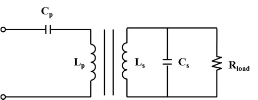
Matching the Tx-Rx is necessary to send as much of the output power of the coupler as possible to the receiver load. There are four basic structures for the loosely coupled inductive power transfer (LCIPT) system used for the Tx-Rx matching network: serial-to-serial (SS), serial-to-parallel (SP), parallel-to-parallel (PP), and parallel-to-serial (PS). As shown in Fig. 8, we use the SP structure for Tx-Rx matching because it alleviates the load variations of the receiver.
From various studies [11-13], we know that
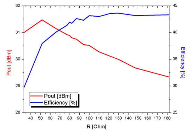
Fig. 9 shows the measurement results to determine the maximum efficiency of the overall system. We use a variable resistor as a load of the circuit to compute the
III. IMPLEMENTATION AND MEASUREMENT
Generally, a network analyzer is widely used in the RF circuits design in the 300 kHz to several GHz frequency band. However, our wireless charging system is implemented at a frequency of 125 kHz, which is based on the
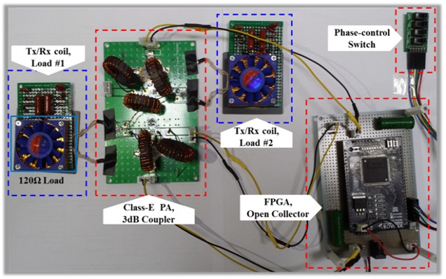
Fig. 10 shows the implementation setup of our reconfigurable system. It is composed of a FPGA controlled by a phase-control switch, two open collectors, two class-E power amplifiers, a four-port power combiner (i.e., a 3-dB coupler), and two pairs of Tx/Rx coils. A four-port quadrature power combiner is implemented with a chip capacitor and a transformer using the Amidon Corporation FT114-61 core considering its size limit [10].
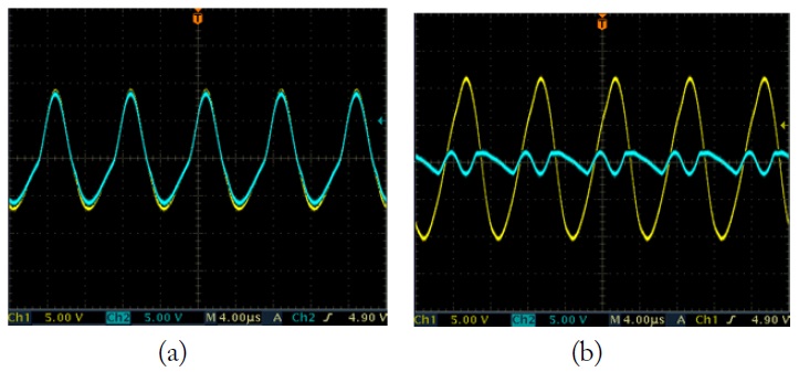
We show the voltage waveform according to the input phase control in Fig. 11. As expected, when we input the different phase, as shown in Fig. 11(b), we can see a 2:0 output in the case of the 90° phase lag.
We measure the
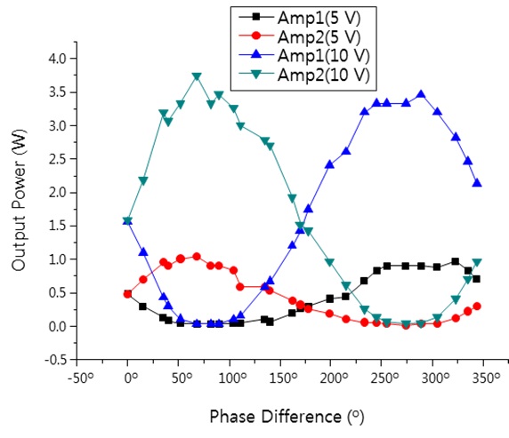
Moreover, we can variably control the total power of transmitter using the DC bias of the drain input of the amplifier. For example, 5 V and 10 V in DC bias have different total output power.
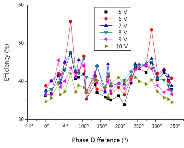
We calculate the power efficiency of a DC–DC conversion according to the variable input phase from zero to 360°, as shown in Fig. 13. From this figure, we can see that the power transfer efficiency is maximized at 6 V of DC bias, which does not coincide with the condition of maximum
We suggest a new schematic using a 3-dB coupler to transmit RF power to two receivers selectively. While several previous schemes to support multiple receivers mainly used the hardware-switched method, our scheme adopts a soft power-allocating method, which has the advantage of variable power allocation in real time to each receiver. Using our scheme, we can split the charging area and focus the wireless power on the target areas. We believe this is a new approach for controlling the power amplifier output softly to support multiple receivers.
In the future, we need to research a mechanism to detect the exact location of the receiving coil to maximize the transmitting power efficiency.