Imaging radar uses radio waves to generate an image of a distant target. Compared to conventional optical imaging systems, radar-based imaging can detect a target regardless of weather or time of day. Although the resolution of the target image is lower than with optical imaging, radio waves can penetrate objects. Therefore, radar-based imaging is suited to security applications, because the system can detect a target hidden behind an obstacle. This type of radar system can be classified as through-the-wall radar [1-3].
Several through-the-wall imaging systems have been researched; however, these are dedicated to a specific frequency band that determines the characteristics of the system. For example, the S-band (2–4 GHz) is useful for detecting a target in a lossy medium, since the S-band signal has good penetration characteristics. However, it also has the drawback of limited image resolution due to its relatively low frequency. On the other hand, the X-band (8–12 GHz) can achieve finer resolution than the S-band, but the detection range of the target is restricted due to its high loss. Thus, a dual-band imaging system is an attractive alternative, since it can flexibly select a suitable frequency according to the situation [4].
In this paper, an imaging radar receiver is designed as part of a dual-band through-the-wall imaging radar system. This receiver front-end can operate in the S-band or X-band, and has the characteristic of attenuating wall-reflected waves when the target is located behind a wall. To reject unwanted reflected waves, a high-pass filter is designed as a key part of the receiver. The filter has reconfigurable frequency response by changing the transconductance of the circuit. In Section II, the design of the overall imaging radar receiver system is described. Section III presents the implementation of the reconfigurable high-pass filter. Section IV presents measurements obtained from the fabricated receiver system, and Section V concludes the paper.
II. IMAGING RADAR RECEIVER DESIGN
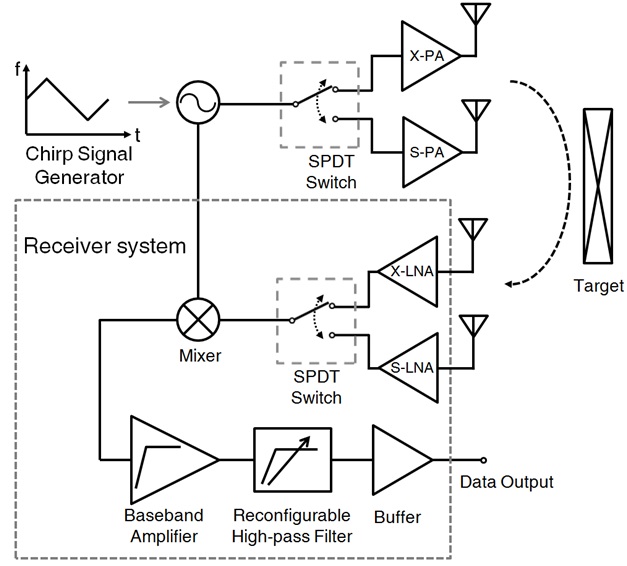
The proposed receiver system of a through-the-wall imaging radar is shown in Fig. 1. The input frequency bands of the receiver are S-band and X-band. The input signal travels from the antenna, and is amplified by a low-noise amplifier (LNA). The antennas are dedicated to one frequency band, so the RF parts of the receiver are designed for each band separately. A switching device is used to select the frequency band electrically. The amplified signal is applied to a mixer and directly downconverted to the baseband. The mixer has wideband characteristics to handle the dual-band input, and the receiver shares the circuit from the mixer stage to the baseband. The local oscillator (LO) signal of the mixer is a frequency-modulated continuous-wave (FMCW) signal, which comes from the transmitter chirp generator.
In an FMCW imaging radar system, the transmitted wave is reflected from the target and enters the receiver antenna. The time-delayed received signal and the transmitted signal are multiplied in a mixer to produce a baseband beat frequency, which is proportional to the distance from the target [5]. When the target is located behind a wall-like obstacle, the wall-reflected wave appears at a lower frequency than the target-reflected wave. Therefore, the system requires a filter to detect the target on the other side of the wall [1, 6]. Moreover, if there is insufficient isolation between the transmitting and receiving antennas, the transmitted signal directly enters the receiver and generates a large baseband signal. This directly-coupled signal must be rejected, since the large baseband signal can saturate the receiver circuits. To reject the direct coupling signal and the wall-reflected signal, the filtering characteristics of the receiver become important.
In [1], a bandpass filter is used to reject unwanted signals. However, since the implemented filter has a fixed frequency response, the system operation should be adjusted to the filter specification. The receiver system in [1] employs heterodyne architecture to adjust the intermediate frequency (IF) to the center frequency of the filter. The radar system in [6] uses a bank of bandpass filters for rejecting the unwanted signal, and an appropriate filter block is selected depending on the distance to the wall and the target. Rather than adjusting the system operation to the filter specification or using a bank of filters, this paper proposes a receiver with reconfigurable high-pass filter to reject the unwanted signal.
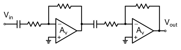
The proposed filtering topology employs a high-pass filter to reject the direct coupling signal and the wall-reflected signal. The baseband signal of the mixer output passes through the amplifier stage shown in Fig. 2. The amplifier stage applies a second-order high-pass filter to reject the direct coupling signal. The distance between the transmitting antenna and the receiving antenna generates a direct coupling signal at a frequency below 100 kHz. Therefore, the cutoff frequency is set to 100 kHz, and this baseband amplifier also amplifies those signals higher than the cutoff frequency, with a gain of 15 dB.
Even if the direct coupling signal is rejected, the wall-reflected wave remains. Therefore, an additional high-pass filter is necessary to attenuate the wall-reflected wave. This filter should be designed to be able to control its cutoff frequency, since the distance between the radar system and the wall and target can vary.
This additional high-pass filter, with its configurable cutoff frequency, is located after the baseband amplifier stage. The cutoff frequency can be adjusted to attenuate the wall-reflected wave and preserve the target-reflected wave. The output signal of the filter is applied to the baseband buffer circuit in Fig. 1, and the buffered signal becomes the final baseband voltage signal.
The resolution of the dual-band radar system is set to 75 cm for the S-band and 25 cm for the X-band. To achieve this resolution, a transmitting FMCW signal bandwidth of 200 MHz at the S-band and 600 MHz at the X-band are needed, and the receiver has to cover the required bandwidth. The X-band chirp signal generator can be implemented by a digital phase-locked loop (PLL) in [7], which has a chirp signal bandwidth of 600 MHz with center frequency of 9.2 GHz. The S-band chirp signal can be obtained using a divide-by-three circuit at the output of the X-band chirp signal generator. The target range is 3.5 m to 20 m from the radar system. The target detection range sets the cutoff frequency of the high-pass filter, which becomes 0.7 MHz to 2.4 MHz. Since this radar system assumes that the distance from the system to the wall is known, the high-pass filter can be adjusted to appropriate cutoff frequency.
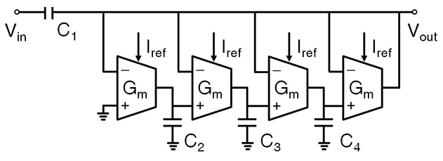
III. DESIGN OF RECONFIGURABLE HIGH-PASS FILTER
To attenuate the wall-reflected wave, a reconfigurable
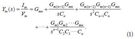
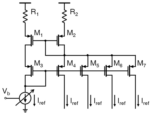
A high-order admittance synthesis method for high-pass filter formation is illustrated in Fig. 3. With input voltage of

Adding capacitor
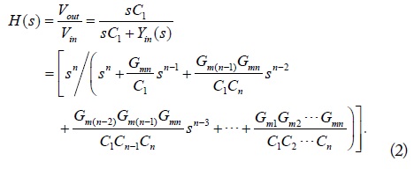
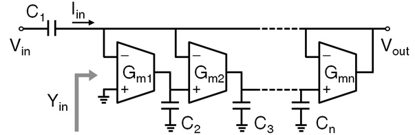
A fourth-order high-pass filter (Fig. 4) is designed by Eq. (2). If the transconductor circuits used in the filter have the same transconductance value (

where the normalized coefficients of the transfer function are
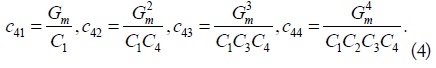
Eqs. (3) and (4) show that the frequency response of the high-pass filter can be scaled proportionally by changing the
The
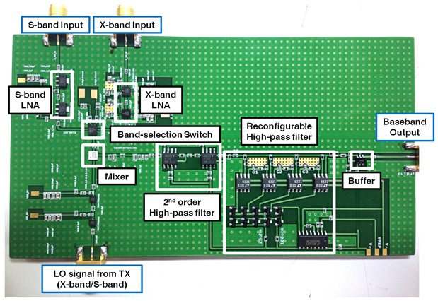
A dual-band imaging radar receiver was fabricated with reconfigurable high-pass filter. The receiver was implemented on an FR-4 printed circuit board (PCB) and consists of commercial devices. The size of the receiver is 13.7 cm × 7.5 cm. Fig. 6 shows a photograph of the receiver. The VDDs for the commercial devices are 3.5 V and 5 V.
The LNAs of each band are cascaded to have appropriate gain at the RF and low noise figure. The X-band LNA is selected to have higher gain than the S-band LNA, since the X-band signal experiences higher loss. A single-pole double-throw switch is used to select the RF input frequency path. The wideband mixer covers the S-band and X-band signals. The baseband amplifier stage in Fig. 2 is implemented, and commercial device OPA211 is used as the operational amplifier. In the reconfigurable high-pass filter, LT1228 devices are used as the transconductors. The reference current source in Fig. 5 is realized by a digital-to-analog converter (DAC) with current output. The transistor
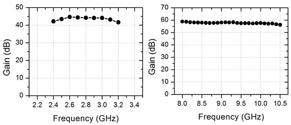
Frequency responses measured from the receiver are shown in Fig. 7. Single-tone RF and LO signals are applied to the receiver, and the baseband signal at 5 MHz is measured. The S-band shows 44.3 dB gain at 2.8 GHz. In the X-band, gain reaches 58 dB and maintains a flat response over a wide frequency range. In both frequency bands, the desired bandwidths of 200 MHz and 600 MHz are achieved.
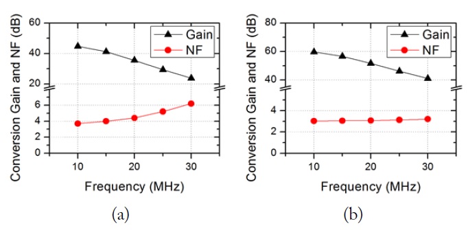
Fig. 8 shows the conversion gain and noise figure (NF) measurements by sweeping the baseband frequency. The minimum NFs of the receiver in each band are 3.7 dB and 3.02 dB, respectively.
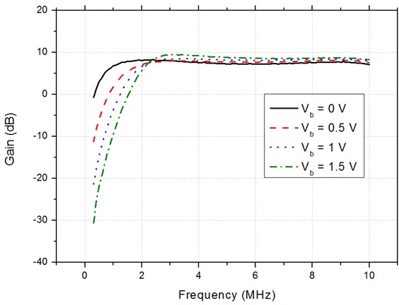
The frequency response of the reconfigurable high-pass filter part is shown in Fig. 9. The graph shows the change of cutoff frequency with the control of the bias voltage. The cutoff frequency of the filter can be tuned from 0.7 MHz to 2.4 MHz, with bias voltage of 0 V to 2 V.
The location of the target and the wall are assumed for two cases. The first case assumes the wall is located less than 1.5 m away, and the target ranges from 7 m to 20 m. The second case sets the wall’s location at 1.5 m to 4 m, and the target from 10 m to 20 m. The filter with bias voltage of 0.5 V corresponds to the first case, and the bias voltage of 1.5 V corresponds to the second case. In both cases, the attenuation of the wall-reflected wave exceeds 20 dB, compared to the target-reflected wave.
A dual-band receiver of a through-the-wall FMCW imaging radar system was designed, and a reconfigurable high-pass filter was implemented as a key part of the receiver. The high-pass filter stage is designed using a high-order admittance synthesis method, and consists of transconductor circuits and capacitors.
A reconfigurable high-pass filter-based receiver system was designed, which can operate at S-band and X-band frequencies. The high-pass filter can be tuned to reject wall-reflected waves at low frequencies, enabling effective target detection.