A resistive and capacitive (RC) microwave absorber with a layer thickness less than a quarter of a wavelength is investigated based on closed-form design equations, which are derived from the equivalent circuit of the RC absorber. The RC absorber is shown to have a theoretical 90% absorption bandwidth of 93% when the electrical layer thickness is 57° (about λ0/6). The trade-offs between the layer thickness and the absorption bandwidth are also elucidated. The presented formulation is validated by a design example at 3 GHz. The RC absorber is realized using a silver nanowire resistive rectangular structure with surrounding gaps. The measured 90% absorption bandwidth with a layer thickness of λ0/8 is 76% from 2.3 GHz to 5.1 GHz in accordance with the theory and EM simulations. The presented design methodology is scalable to other frequencies.
As various applications in the area of communication, medicine, and defense, among others, are being developed and deployed rapidly, the demand for microwave absorbers is also increasing. Microwave absorbers are used for anechoic chambers [1], mobile phones, EMI/EMC problems, stealth air planes [2], and other applications. Particularly, they are required to minimize the hazards of EMP attacks.
The current commercial absorbers are usually made of ferrite materials, which are expensive and bulky. To replace these materials, many other types of absorbers have been introduced and developed. Recent advancements in metamaterial research have opened the possibility for metamaterial absorbers (MA) [3–5]. The literature shows that MAs can be realized very thinly, but their bandwidth is still narrow. Thus, a double layer may have to be used [5].
A conventional absorber is the Salisbury screen [6]. The Salisbury screen is made of a 377-Ω resistive film placed at a distance of quarter wavelength above a conducting plane. The thickness of the absorber is relatively thick at low frequencies because of the required spacing of
In this paper, the absorbers with a layer thickness less than a quarter of a wavelength are designed using a resistive and capacitive (RC) screen. The reason why the capacitive RC screen is employed is that the impedance of the layer, which has a thickness less than a quarter of a wavelength, is inductive. Convenient design equations are derived using a proper equivalent circuit. The provided design equations are useful for synthesizing any particular absorber at a specific frequency, and they also give us physical insight into the bandwidth trade-offs between the thick and thin absorbers. Particularly, the bandwidths of the RC absorbers are compared with those of the metamaterial-type absorbers. Finally, for the validity of the formulation, an RC absorber made of a silver nanowire (AgNW) resistive film is designed at 3 GHz, fabricated, and measured. Comparisons and discussions are then conducted.
II. DESIGN OF THIN MICROWAVE ABSORBERS
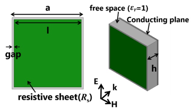
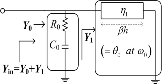
The proposed absorber is composed of an RC screen and a conducting plane separated by a distance of less than a quarter of a wavelength. Fig. 1 shows the equivalent circuit of the RC absorber, where

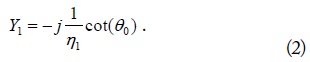
and the admittance
For the input admittance match of the absorber to free space, we require

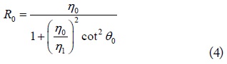
By separately equating the real and imaginary parts of (3), we obtain the unique solutions of

and
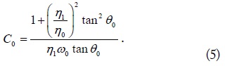
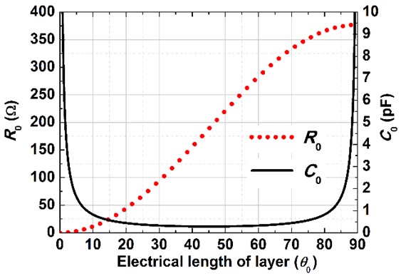
Fig. 2 illustrates the required circuit values of
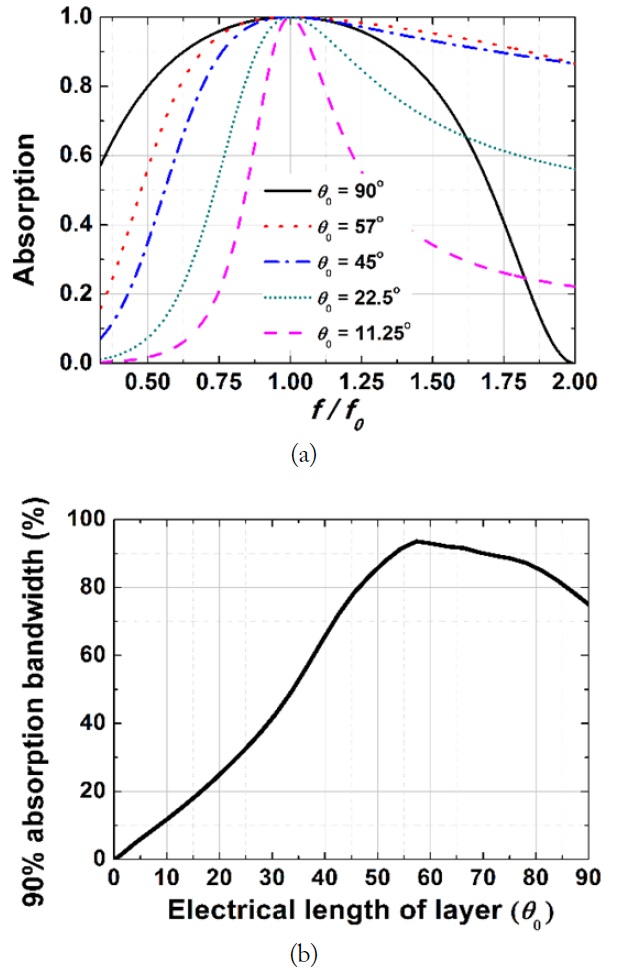
Fig. 3(a) shows the absorptions (= 1–|
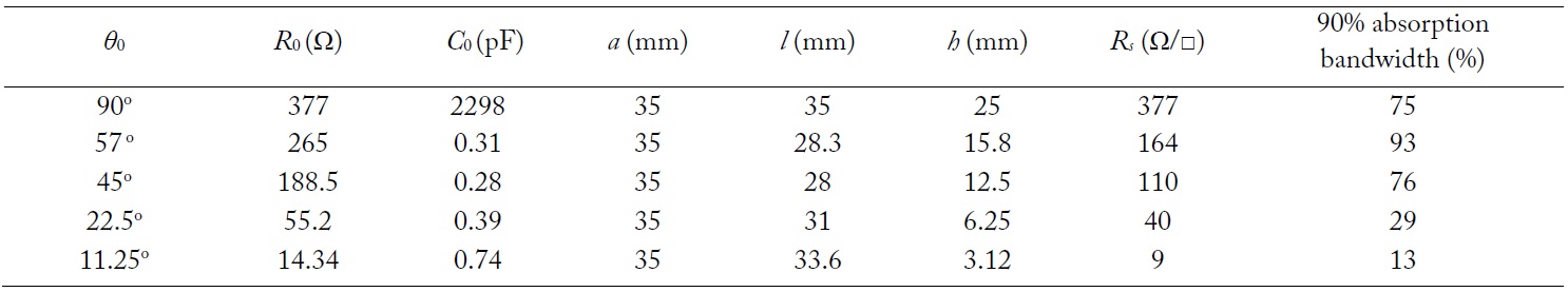
Fig. 4 illustrates a unit structure of the RC absorber with dimensions determined at a design frequency of 3 GHz using EM simulations for the case of

Designed absorber parameters and 90% absorption bandwidths for different air-spaced layer electrical lengths at 3 GHz
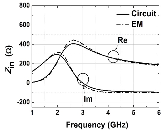
Fig. 5 demonstrates the real and imaginary parts of
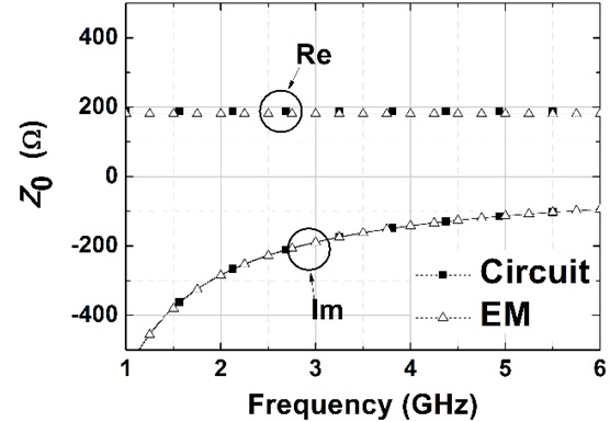
In Fig. 6, the EM-simulated input impedance
III. FABRICATION AND MEASUREMENTS
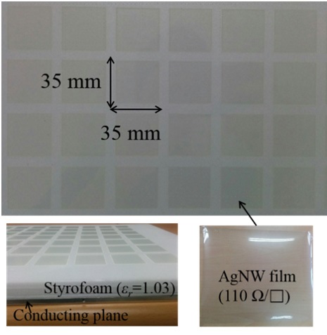
Fig. 7 shows a photograph of the fabricated RC absorber made of AgNW resistive film. The AgNW film with 110 ±4 Ω/□, produced by Cosmo AM&T (www.cosmoamt.com), was cut by a laser-cutting machine. The whole patterned film was then attached to a Styrofoam layer. The unnecessary part was detached later. One unit is composed of a square-shaped AgNW film, a Styrofoam layer of 12.5 mm (
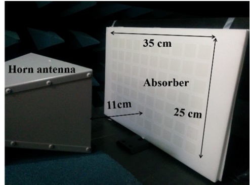
Fig. 8 presents the measurement setup to estimate the absorptions of the fabricated absorber with one horn antenna. The size of the fabricated absorber is 35 cm (10 units) × 25 cm (7 units). The measurements were conducted to change the distance between the standard horn antenna and the absorber from 3.5 cm to 23 cm. Although the absorber is placed somewhat in the near field, the following extraction procedures have been found to give closer results than the EM-simulation results [11].
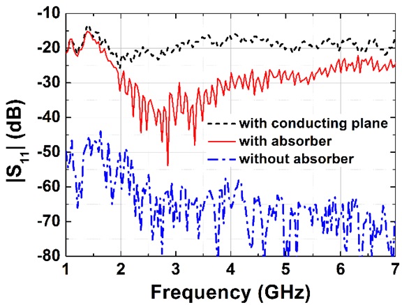
Fig. 9 illustrates the measured reflection coefficients of the horn antenna in free space (
This estimation removes the effects of the used horn antenna and minimizes the effects of the used near-field measurements. The measured absorption is calculated using (1–|
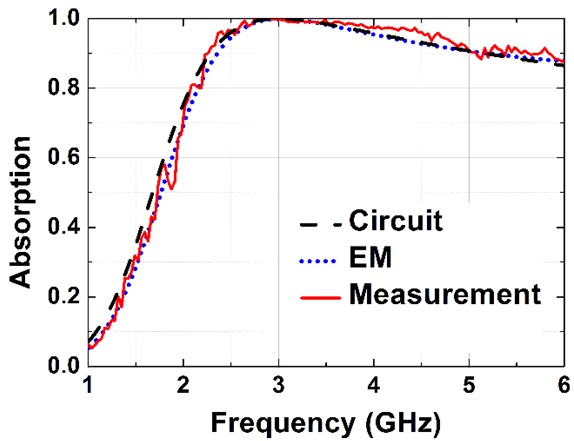
In Fig. 10, the measured absorption is shown to agree well with the theoretical (or circuit-simulated) and EM-simulated absorptions. The measured 90% absorption bandwidth is approximately 76% (2.3–5.1 GHz) with a complete absorption at the design center frequency of 3 GHz.
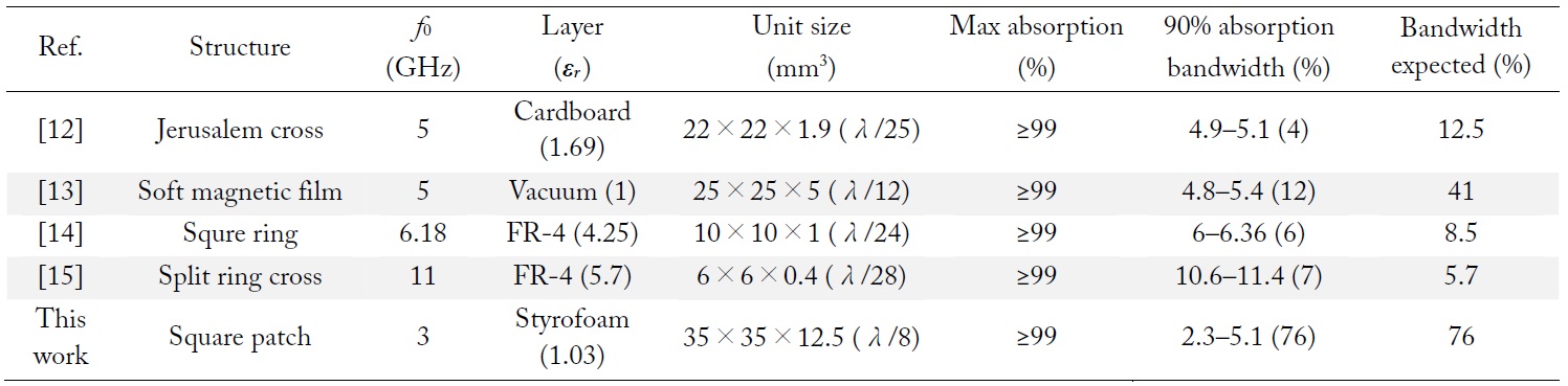
In Table 2, the absorption characteristics of the thin absorbers in [12–15] are compared with those theoretically expected by the proposed design method. Except for the case of [15] in which the measured bandwidth of 7% is wider than 5.7%, the bandwidth characteristics of the rest are shown to be at best comparable with or even far worse than those of the presented simple RC absorbers although diversified structures have been employed.
[Table 2.] Comparison of absorber characteristics with those of this work

Comparison of absorber characteristics with those of this work
An RC absorber with a layer thickness of less than a quarter of a wavelength has been examined from a simple equivalent circuit. Closed-form design equations have been derived and presented. The validity of the presented formulation has been demonstrated by a design example for the RC absorber at 3 GHz. The RC absorber has been designed, fabricated with AgNW resistive film, and measured. The absorber is shown to offer a 90% absorption from 2.3 GHz to 5.1 GHz (76%) with a layer thickness of 1/8 wavelength. The proposed design methodology is scalable to other frequencies.