This paper proposes a reconfigurable microstrip diplexer, also known as a switchplexer, for use with single-switch operation of frequency band and output path. The proposed switchplexer is composed of a rectangular ring resonator and a switch on a shorting pin, which is inserted between the ring resonator and the ground plane. The rotated main current distributions occurring at different switch statuses provide the diplexer’s different operating bands and different output ports. The performance of the simply designed switchplexer is successfully demonstrated via simulation and measurement.
Diplexers are an essential component of modern wireless communication systems, where fast progress in wireless and mobile technology has created a demand for multi-band and multi-functional capabilities. Microstrip diplexers, due totheir low profile, light weight, low cost, and easy integration with other front-end circuitry, have recently become more popular. In the past, numerous diplexers have been proposed [1–4]. However, these previous diplexers have all had fixed frequency bands. As multiband communication systems have been developed, multiband filters and tunable filters have been proposed [5–7]. The technique for multi-band and multi-functional capabilities using the diode and switch has also been found to be useful in other microwave applications, such as for use with reconfigurable antennas [8,9]. Recently, the diplexer and switch in time-division communications systems were combined into one device, called the switchplexer [10–12].
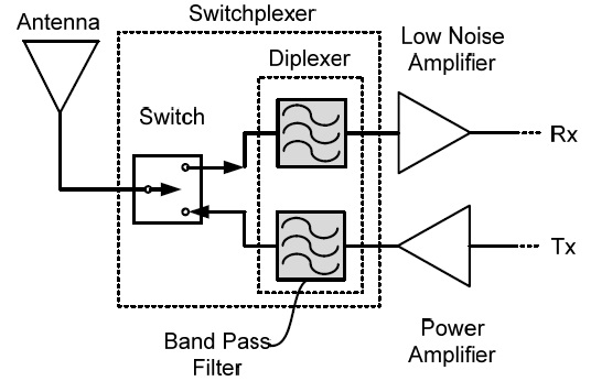
Fig. 1 shows the concept of the switchplexer [12], which integrates both the switch and the diplexer. The switch can change the signal path between the receiving and transmitting signals, as described in [11,12], or it can change the signal path between the two receiving signals with different bands, as shown in [10]. The diplexer consists of two or more bandpass filters. The benefit of the switchplexer is that it decreases the insertion loss and the amount of space occupying, making even the design process easier [10].
This paper proposes a new microstrip switchplexer that can change the current distribution electrically on the rectangular ring resonator using only single-switch operation.
The elements contained in the switchplexer depend on the system configuration to be implemented. The switchplexer shown in [11] integrates the switch, diplexer, and even the balanced-to-unbalanced (balun) transformer. Meanwhile, the switchplexer studied in [12] integrates the switch, diplexer, and low-noise amplifier (LNA). The switch integrated in [10] is the double-pole double-throw (DPDT) switch, and it is connected to two antennas for multiple-input multiple-output (MIMO). The proposed switchplexer in this paper contains the switch and diplexer consisting of two band-pass filters.
The switchplexer proposed in this paper has been designed for application with low-cost time-division systems. For this reason, a one-wavelength microstrip resonator was utilized with one switch. This accomplished a simple and low-cost switchplexer. The diplexer of previous work described in [8–11] was configured with the cascaded filters. However, the diplexer of the proposed switchplexer is the simple one resonator. This kind of switchplexer utilizing a one-wavelength microstrip resonator and a single switch has been reported, as far as we know. The simulation and measurement results indicate the validity of the proposed technique.
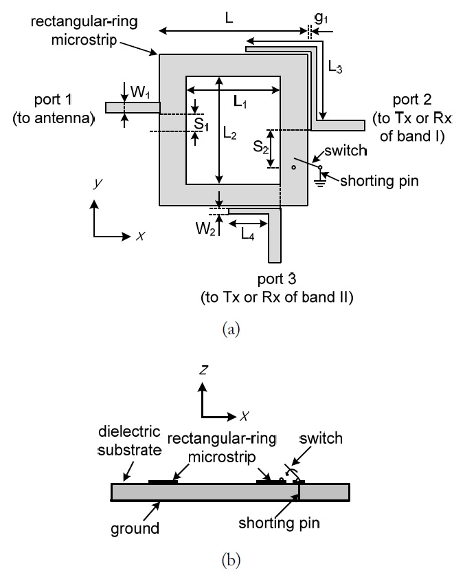
The geometry of the proposed microstrip switchplexer is shown in Fig. 2. As shown in Fig. 2(a), the simple reconfigurable switchplexer consists of a square-ring resonator and a switch on a shorting pin.
Port 1 is connected to the antenna, and port 2 and port 3 are connected to the transmitting or receiving system by band I or band II, respectively. Meanwhile, port 1 is directly connected to the diplexer, and the two output ports (port 2 and port 3) use parallel couple lines for tight coupling between the rectangular resonator and the feed lines. The gap and width of the coupling microstrip have been optimized by manual tuning, resulting in
The shorting pin is inserted between the ground plane and the rectangular ring resonator, as shown in Fig. 2(b). The radius of the shorting pin is 0.5 mm. The on/off connection between the microstrip and the shorting pin has been done using the switch operating by supplying voltage.
The circumferential length of the ring is one wavelength. Therefore, the lateral outer length of the square ring is
Here, the relative dielectric constant, loss tangent, and thickness of the dielectric substrate is ε
The positions of port 1, 2, and 3, as marked in Fig. 2(a), are closely related to the operating principle, as described in next paragraph. This results in
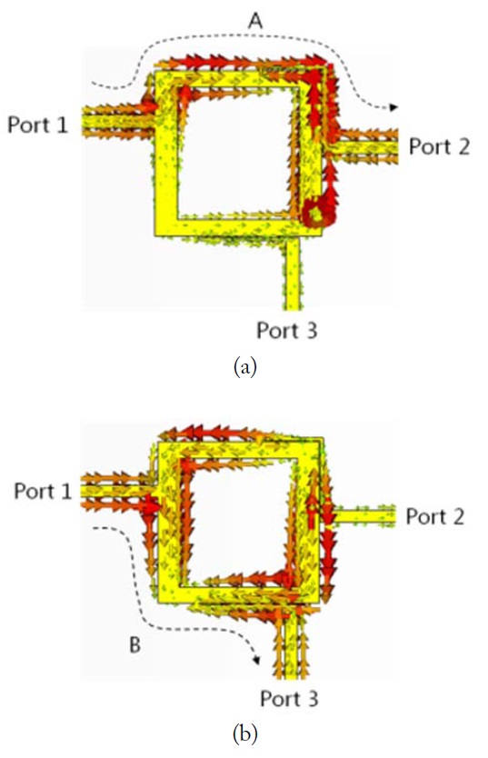
The operating principles can be explained using Fig. 3, which shows the surface current distributions of the switchplexer according to the different switch status. The strong current distribution is marked with the large arrow, while the weak current distribution is marked with the small arrow.
The idea proposed in this paper came from the unloaded ring and loaded-ring resonators described in [13], where the polarization of the loaded ring is rotated by 90° compared to that of the unloaded ring. Because the rectangular shape is not important, the circular ring can also be used.
In Fig. 3(a), the main current is distributed horizontally at the switch-closed status and coupled with the feed line ofport 2 (path A). This is analogous to the current distribution for the shorting-pin loaded-ring resonator, as shown in [13].
In contrast, at switch-open status, the current distributions are vertically directed; therefore, they are coupled with the feed line of port 3 (path B), as shown in Fig. 3(b). This is analogous to the current distribution for the unloaded-ring resonator, as shown in [13].
These results demonstrate that the current path can be controlled electrically using single-switch operation.
III. SIMULATED AND MEASURED RESULTS
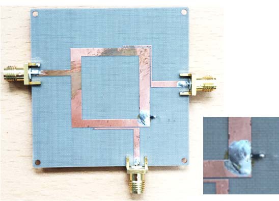
The simulation has been performed using a three-dimensional electromagnetic simulator from CST Microwave Studio. A prototype switchplexer was fabricated and measured to verify the proposed switchplexer characteristics. The topology of the fabricated reconfigurable diplexer is shown in Fig. 4. The Tx and Rx resonator have been designed to provide passbands centered at 2.14 GHz and 2.24 GHz, respectively. The diode for the shorting function was soldered between the microstrip patch and the ground. The utilized PIN diode is SMP1345-079; this diode was produced by Skyworks.
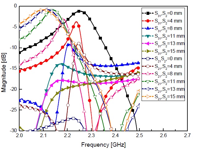
Fig. 5 shows the investigated shorting pin position for the optimal design of the switchplexer. Here, the switch is closed. The shorting pin is also offset by the
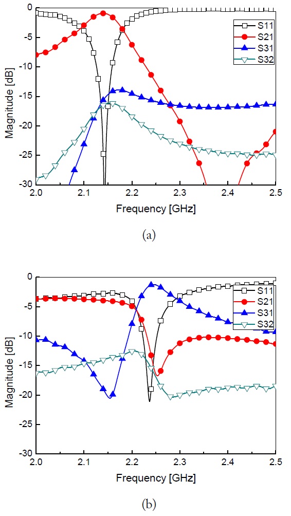
Fig. 6 shows the simulated reflection and transmission coefficients for the switch-open and switch-closed statuses. In the closed switch, the prototype obtained an insertion loss of 0.9 dB at 2.14 GHz. The 3-dB bandwidth was about 90 MHz and the isolation between port 2 and port 3 was 16 dB, as shown in Fig. 6(a). In the open switch, the insertion loss of 1.25 dB was achieved at 2.24 GHz. The 3-dB bandwidth and the isolation were 90 MHz and 15 dB, respectively, as shown in Fig. 6(b).
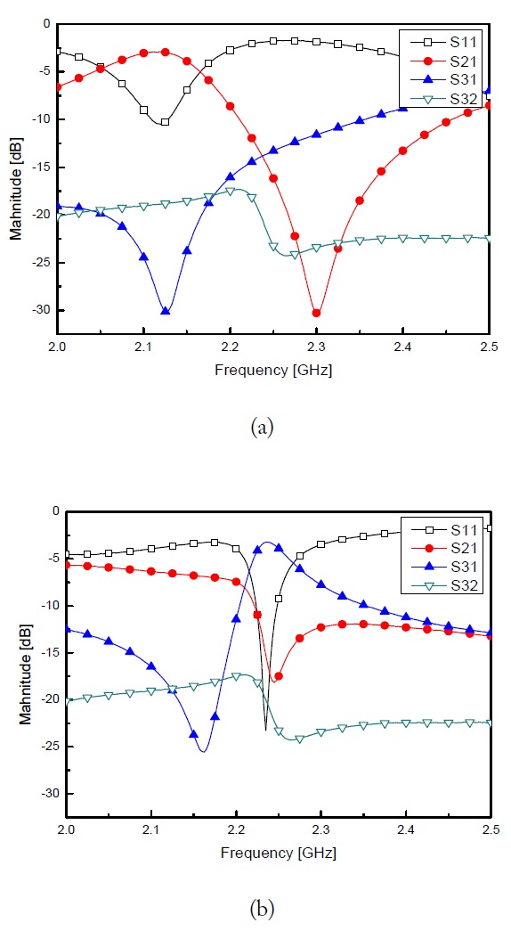
Fig. 7 shows the measured results for the switch-open and switch-closed statuses. DC-feeding was configured using a ZFBT-4R2GW-FT+ bias-tee (Mini-Circuits, Brooklyn, NY, USA). The measured insertion loss was 2.22 dB at 2.12 GHz for the switch-closed status and 2.59 dB at 2.24 GHz for the switch-open status. The measured isolation between port 2 and port 3 was 17.1 dB and 19.9 dB for the switchopen and switch-closed statuses, respectively. The 3-dB bandwidth was 153 MHz for the switch-closed status and 65 MHz for the switch-open status. Strong agreement was observed between the measured and simulated results. The insertion loss of the fabricated switchplexer was not small, but the simulated switchplexer had a small value that could be utilized in a real application. This difference might be due to the modeling error caused by the PIN diode and shorting pin.
This study proposed a reconfigurable microstrip diplexer, called a switchplexer, which changed its current distributions electrically with only single-switch operation at different bands of 2.14 GHz and 2.15 GHz. These frequencies are only designed for verification the proposed switchplexer, but easily tuned for the commercial frequency band adjusting the parameter of the ring resonator. An isolation level of more than 15 dB was also obtained for both the switch-open and switch-closed statuses. The simple and low-cost design for a switchplexer using only a rectangular microstrip line resonator and a switch may be suitable for time-division communication systems.