This paper presents the design of a negative group delay circuit (NGDC) using the filter synthesis approach. The proposed design method is based on a frequency transformation from a low-pass filter (LPF) to a bandstop filter (BSF). The predefined negative group delay (NGD) can be obtained by inserting resistors into resonators. To implement a circuit with a distributed transmission line, a circuit conversion technique is employed. Both theoretical and experimental results are provided for validating of the proposed approach. For NGD bandwidth and magnitude flatness enhancements, two second-order NGDCs with slightly different center frequencies are cascaded. In the experiment, group delay of 5.9±0.5 ns and insertion loss of 39.95±0.5 dB are obtained in the frequency range of 1.935–2.001 GHz.
Most media exhibit a normal propagation characteristic called subluminal velocity, where the speed of propagation of individual time-harmonic components is slower than the speed of light,c, in vacuum at all frequencies. However, in a specific and narrow frequency band of signal attenuation or at an anomalous dispersion frequency, the group velocity is observed to be greater than
One example of the concept of superluminal velocity is the negative group delay (NGD); this refers to the phenomenon whereby an electromagnetic wave traverses a medium in such a manner that its amplitude envelope is advanced rather than delayed [6]. Recently, many studies have designed negative group delay circuits (NGDCs) and used them in practical applications such as enhancing the efficiency of a feed-forward amplifier [7], shorting delay lines [8], realizing non-Foster reactive elements [9], and minimizing beam-squint problems in series-fed antenna arrays systems [10].
The conventional design method of active and passive NGDCs is based on only single
In this study, a filter synthesis approach is applied to design an NGDC. In this proposed method, circuit element values are obtained from low-pass filter (LPF) prototypes by applying a frequency transformation.
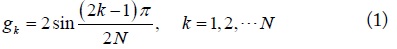
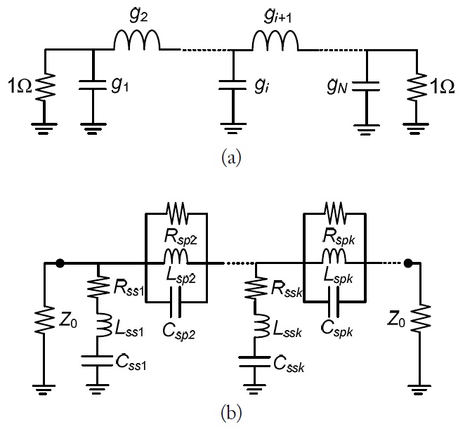
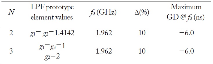
Fig. 1(a) shows the Butterworth LPF prototype. The element values of the LPF are obtained as follows [19].

where
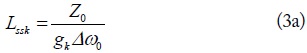
where


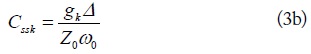
where
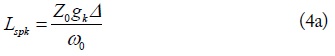
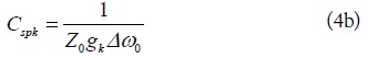
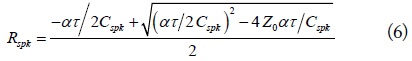
The resistors are inserted into the shunt and series resonators to obtain the required NGD. The values of these resistors are obtained by analyzing the shunt-series and series-parallel branch elements [18], respectively. The resistances in the shunt-series branch of the NGDC for the required NGD are given as follows.
where

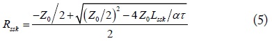
A correction factor
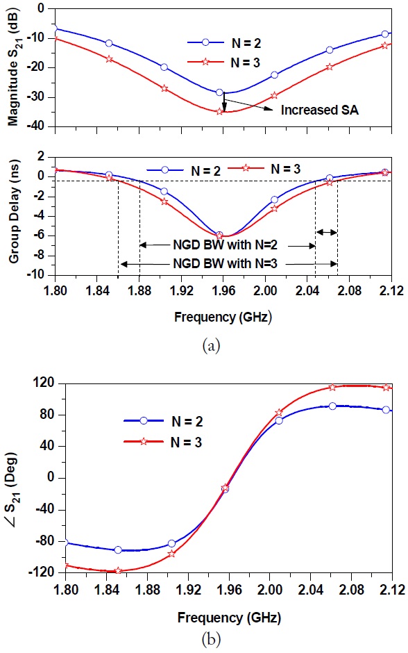
Fig. 2 shows the synthesized results of the NGDC with different numbers of stages
[Table 1.] Specifications of negative group delay circuits
Specifications of negative group delay circuits
[Table 2.] Element values of negative group delay circuits (NGDCs) with GD=-6 ns
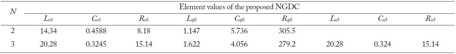
Element values of negative group delay circuits (NGDCs) with GD=-6 ns
[Table 3.] Calculated NGD BW and SAmax for different numbers of filter stages

Calculated NGD BW and SAmax for different numbers of filter stages
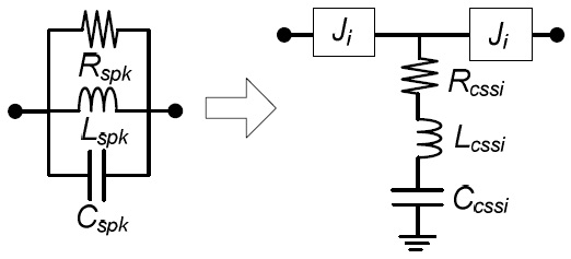
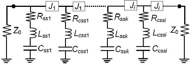
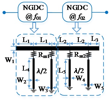
The proposed NGDC shown in Fig. 1(b) consists of both shunt-series (
To overcome this problem, the circuit conversion technique can be applied to convert the series-parallel lumped elements (


Theoretically, the value of the
III. SIMULATION AND EXPERIMENTAL RESULTS
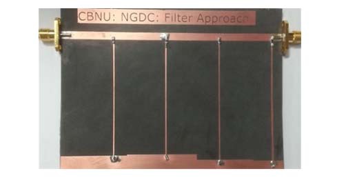
To validate the proposed design method, a second order NGDC was designed and fabricated on a substrate with dielectric constant (
As shown by the results in the previous sections, the NGD bandwidth of the proposed circuit is narrow. One of the ways to increase the NGD bandwidth is to increase
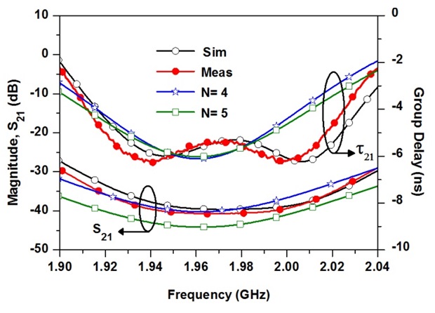
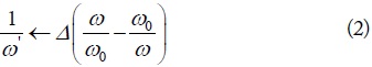
Fig. 6 shows the simulation and measurement results of the fabricated cascaded two-stage NGDC and comparison with NGDCs with
These results also show that the NGD bandwidth and magnitude flatness are wider than those of NGDCs with
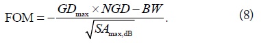
Table 4 shows a performance comparison of the proposed NGDC with those in previous works. Owing to the trade-off among the maximum achieved GD (GDmax), maximum SA (SAmax) and NGD bandwidth (NGD-BW), the figure of merit (FOM) of NGD circuits can be defined as follows.

[Table 4.] Performance comparison of the proposed NGDC with those in previous works
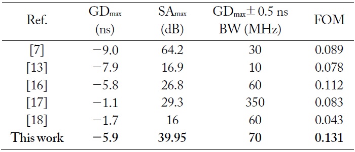
Performance comparison of the proposed NGDC with those in previous works
As seen from Table 4, the proposed NGDC provides the highest FOM and best performance in terms of GD/magnitude flatness even though the SA is higher than of some previously proposed NGDCs [13,16-18].
In this paper, a filter synthesis approach is applied to design a NGDC. The circuit elements of the proposed filter can be obtained from LPF prototype elements. The proposed circuit was implemented with a distributed transmission line using a circuit conversion technique. An experiment was performed to validate the proposed design method. The measurement results agreed well with the simulation results. The proposed NGDC shows the highest FOM, large negative group delay, good magnitude flatness, and wider negative group delay-bandwidth.