A commercial 0.25 μm GaN process is used to implement 6–18 GHz wideband power amplifier (PA) monolithic microwave integrated circuits (MMICs). GaN HEMTs are advantageous for enhancing RF power due to high breakdown voltages. However, the large-signal models provided by the foundry service cannot guarantee model accuracy up to frequencies close to their maximum oscillation frequency (Fmax). Generally, the optimum output load point of a PA varies severely according to frequency, which creates difficulties in generating watt-level output power through the octave bandwidth. This study overcomes these issues by the development of in-house large-signal models that include a thermal model and by applying distributed L-C output load matching to reactive matched amplifiers. The proposed GaN PAs have successfully accomplished output power over 5 W through the octave bandwidth.
A wideband RF power amplifier (PA) is an essential component in many RF applications, such as electronic warfare (EW) systems and security communications. In the past, the traveling wave tube amplifier (TWTA) has been most commonly used to achieve wideband output power above watt levels [1,2]. However, the emergence of GaN PAs raises the prospect of replacing bulky TWTAs with compact solid state power amplifiers (SSPAs) [3]. GaN high-electron-mobility transistors (HEMTs) have several inherent advantages, including high breakdown voltage, high current density, and high saturation velocity resulting from their wide band gap properties [4]. Unfortunately, unlike GaAs or InP HEMTs, GaN HEMTs have a large power dissipation, which causes a prominent self-heating phenomenon that degrades the RF performance of devices [5]. Thus, the self-heating effect must be considered when designing wideband RF GaN PAs. An accurate large-signal model that includes a thermal model therefore becomes an inevitable requirement. Large-signal models provided by the foundry service are still not mature and do not guarantee model accuracy up to frequencies close to the maximum oscillation frequency (
The optimum output load point of an RF PA typically shows severe variation with the frequency. Because of this variation, a conventional output load matching prevents RF PAs from obtaining wideband output power. The output load matching circuits should therefore be designed by taking into consideration the frequency-dependent load variation.
This paper describes the development of in-house large-signal models of a GaN HEMT that include a thermal model. Distributed L-C output load matching is proposed for the design of reactive matched amplifiers. Section II presents the large-signal models, followed by the proposed design of the reactive matching PA in Section III. Experimental results are presented in Section IV.
II. LARGE-SIGNAL MODELING OF THE GAN HEMT
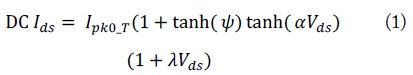
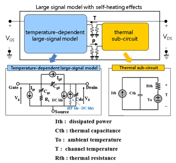
Our in-house models are based on an Angelov model [6,7]. Fig. 1 shows an Angelov model-based GaN HEMT large-signal equivalent circuit including a thermal model. Our inhouse models consist of the Angelov model library supported by Keysight’s ADS 2013 program and thermal sub-circuits [8]. Thermal sub-circuits inform a temperature-dependent large-signal model of the channel temperature raised by Rth. In particular, our in-house models incorporate a nonlinear drain current (


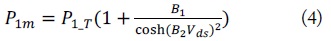


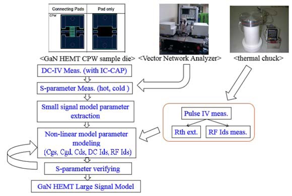
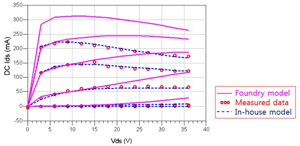
Fig. 2 shows the large-signal modeling procedures. First, DC–IV curves are measured in a device under test (DUT) by an HP 4142B DC source and a Keysight’s IC-CAP program. The sample dies of GaN HEMT, provided by the foundry service, are used as DUTs. The
[Table 1.] Model parameters in nonlinear drain current equations of 6 × 125 μm GaN HEMTs
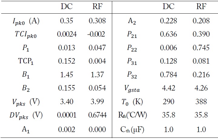
Model parameters in nonlinear drain current equations of 6 × 125 μm GaN HEMTs
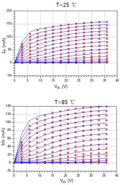
Fig. 3 shows a comparison of the DC–IV curves between the measurements and the models, measured at drain voltages (
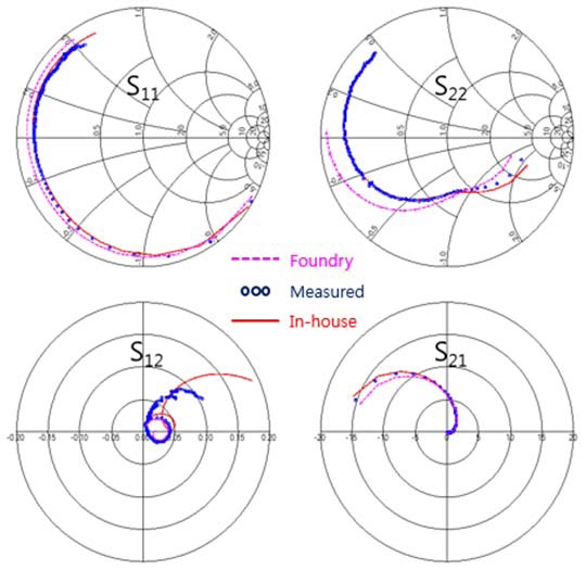
Fig. 5 represents the comparison between the measured
III. DESIGN OF A REACTIVE MATCHED GAN PA
A reactive matched PA is a type of wideband power amplifier that has an octave bandwidth. It purposely decreases the Q-Fig factors by inserting lossy matching components at the gate of the transistors [11-14]. This approach improves the gain bandwidth, while sacrificing peak gain, peak output power, and power efficiency. However, obtaining the wideband output power requires an additional circuit topology in the reactive matched PA design.
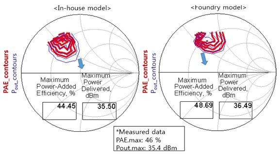
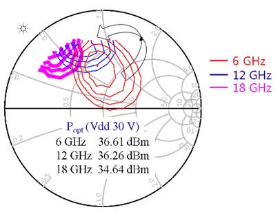
Fig. 7 shows the simulated load pull contour of the 6 × 125 μm GaN HEMTs according to frequencies. As shown in Fig. 7, when the operating frequency increases, the load pull contour rotates in a counterclockwise direction on the Smith chart. Unfortunately, the general output load impedances rotate in the clockwise direction on the Smith chart according to frequencies, which causes the output power characteristics to be very frequency dependent. This prevents the usual PAs from generating uniformly high output power over a wide bandwidth.
We reduce these mismatches between the optimum loads and the output impedances by adopting the L-C resonance technique in the output load matching circuit [15]. First, we set the resonance frequency (in this case, 12 GHz) in the middle of the operating frequency region.
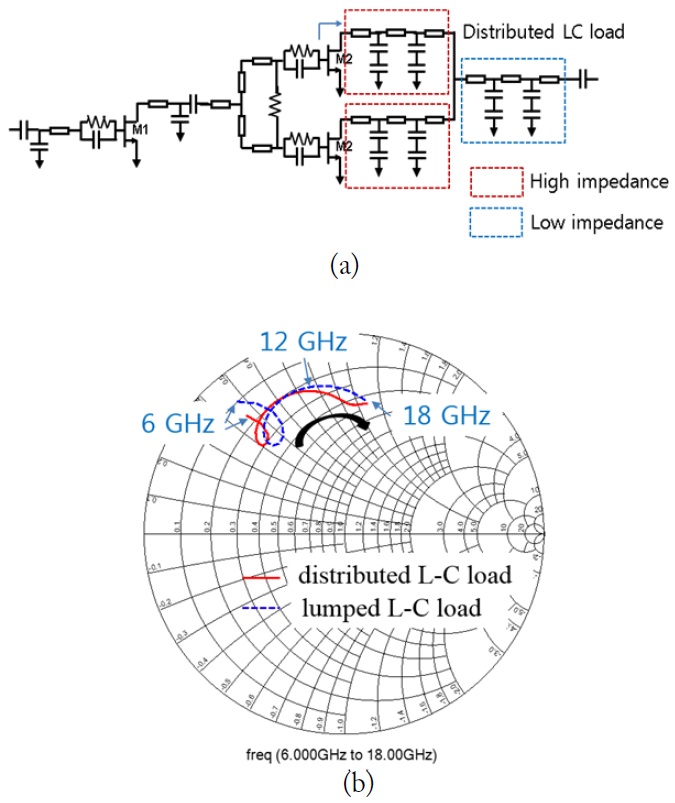
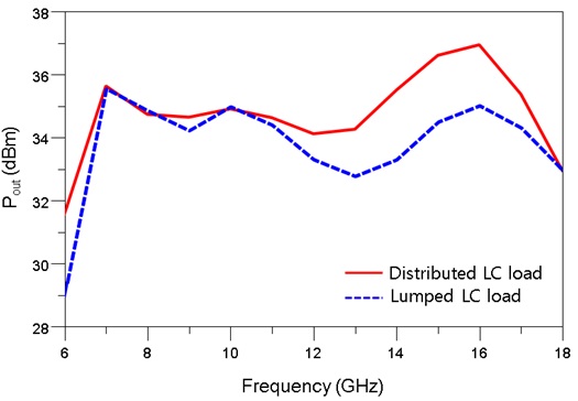
The appropriate value of L and C for resonance is then designed, taking into consideration the length of the micro-strip lines and the size of metal insulator metal (MIM) capacitors. If the capacitance is too large, the power gain will decrease steeply at high frequencies. On the contrary, if the inductance is too large, the layout will be bulky and the MIM capacitors will be too small to be implemented. In this work, the selected values of L and C are 600 pH and 330 fF, respectively. The output load matching circuits are implemented by the distributed L-C components. The distributed L-C components are repeatedly put close behind the output transistors and after combining the two-unit PAs. Micro-strip lines (50 μm wide and 300 μm long) are used as a distributed inductance of about 150 pH. The MIM capacitors (30 μm × 30 μm) are used as a distributed capacitance of about 230 fF. The distributed L-C components bring about a lower Q than is obtained with lumped L-C components [16]. In addition, the use of micro-strip lines of widths, ranging from 20 to 100 μm according to the output load matching section, mitigates the frequency-sensitive output load variation. Both the L-C resonance and distributed components decrease the variation of the output load impedance according to frequencies. Therefore, these methods can bring about a greater improvement in the wideband output power characteristics. The circuit schematic of a two-stage reactive matched PA with the distributed L-C loads is shown in Fig. 8(a). Fig. 8(b) compares the output impedance under the distributed L-C load with the output impedance under the lumped L-C load on the Smith chart. The output impedance under the distributed L-C load passes through a lower Q region that is relatively closer to the optimum loads than it does when a lumped L-C load is applied. Therefore, as shown in Fig. 9, the PAs with the distributed L-C load bring about higher output power than is seen with the lumped L-C load through the wideband frequency region.
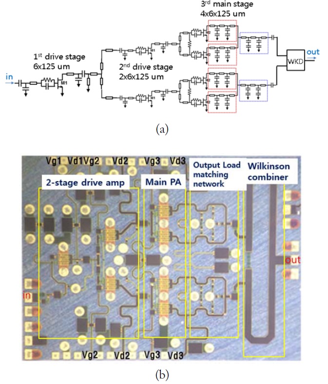
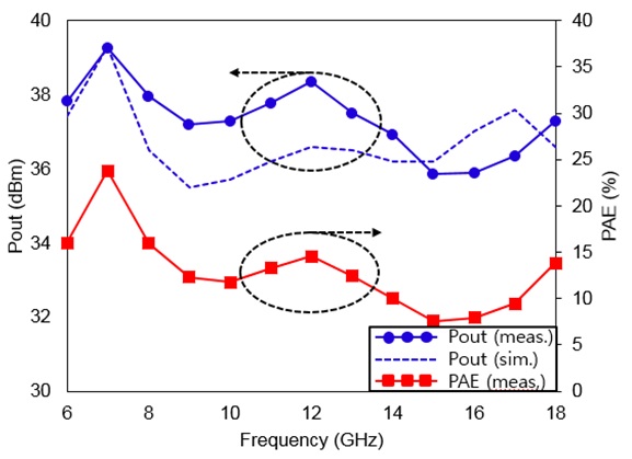
The proposed PA MMIC has been fabricated by a commercial 0.25 μm GaN process. Fig. 10(a) and (b) show the circuit schematic and the chip photograph. The proposed GaN PA is designed as a three-stage reactive matched type. The GaN HEMTs (6 × 125 μm) are commonly used in the drive and main power stage. The output stage consists of the distributed L-C output load matching circuits of Fig. 8(a) and a Wilkinson power combiner.
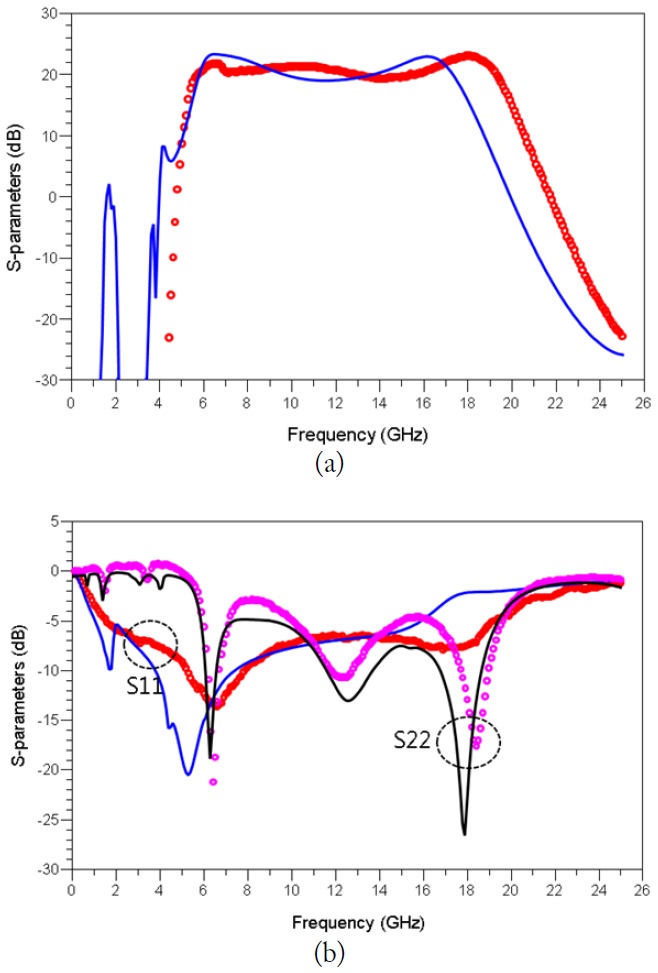
Figs. 11(a) and (b) compare the measured small-signal
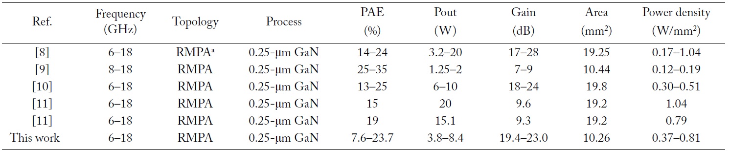
Fig. 12 depicts the measurements of the continuous wave (CW) output power (
The
Table 2 compares the performance of reactive matched GaN PA MMICs. The 0.25-μm GaN process used in this work shows a lower
[Table 2.] Performance comparison table of GAN reactive matched power amplifiers

Performance comparison table of GAN reactive matched power amplifiers
We implemented 6–18 GHz wideband GaN power amplifiers using a GaN HEMT large-signal model that incorporates a thermal model and is based on various measurements. The inhouse GaN HEMT model is effectively used to design a reactive matched PA up to frequencies close to the device’s