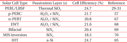
Over the past decade, the annual growth rate of solar photovoltaic (PV) technology is approximately 50%, whereby Si-wafer-based PV technology accounted for approximately 90% of the total production quantity. The material usage for c-Si solar cells has been reduced significantly during the last five years from approximately 16 g/Wp to 6 g/Wp due to an increased efficiency and thinner wafers.
The corresponding reduction of manufacturing costs can be primarily attributed to economy of scale effects and technological progress. The reduced wafer thickness and manufacturing costs mean that the new technologies are very simple, cost effective, and highly efficient. To achieve a high efficiency, it is necessary to reduce both the loss of photo-generated carriers and the loss of sunlight entering into the cell [1].
To improve the effective minority-carrier lifetime, a passivation layer is used to reduce the surface recombination of the photo-generated carriers. An anti-reflection coating (ARC) is used to reduce the optical loss caused by the reflection at the air/c-Si interface. Reducing the electrical losses at the c-Si surface is more challenging than reducing those of optical losses. In this paper, a surface-passivation scheme is reviewed for high-efficiency c-Si-based solar cells.
2. SURFACE PASSIVATION TECHNIQUES
While the application of thinner c-Si wafers as the base material for high-efficiency solar cells has become a trend, corresponding electrical losses at the c-Si surface have become an increasing concern (Fig. 1 depicts the predicted reduction in wafer thickness); consequently, the recombination losses at the semiconductor interface must be minimized. Recombination losses at the semiconductor interface can be reduced by the following two passivation methods: chemical passivation and fieldeffect passivation. The latter can be undertaken using the charge induction in the Si-surface regions by means of a built-in electric field, viz. the front-surface field and back-surface field (BSF). The two passivation methods are discussed in the subsequent section of this paper.
Chemical passivation is achieved by reducing the number of defect states (Dit) that are present at the Si surface, either by the hydrogen passivation provided by plasma deposition or by a forming gas annealing (FGA). Chemical passivation is effective for both n- and p-type c-Si, since it reduces the surface defects by saturating the Si dangling bonds; therefore, the conversion efficiencies of both the n- and p-type c-Si-based solar cells can be improved. This strategy is much more sensitive to the presence of defects at the surface, and is usually carried out by depositing or growing a passivation layer over the c-Si surface.
Apart from chemical passivation, surface recombination can also be reduced by field-effect passivation by depositing a charged layer (for example, SiNx) over the c-Si, or by forming a heavily doped region (for example, BSF at the rear side of the c-Si). BSF can be formed by firing back-contact Al into p-type c-Si, thereby forming a high-low junction (i.e., p+/p). The electric field across the high-low junction prevents recombination by repelling minority carriers toward the bulk of the device; therefore, in terms of p-type c-Si-based solar cells, the electrons flow toward the front surface, and the negative charges in the front-surface regions consequently enhance the photocurrent flow and efficiency.The positive charges near the front surface, however, have a contrary effect, leading to a decrease of the conversion efficiency. For n-type c-Si-based solar cells, positive charges in the front-surface regions and negative chargesnear the rear surface can improve the performance of the solar cell.
The incorporation of fixed charges in the dielectric passivation layer can be achieved by plasma-enhanced chemicalvapor deposition (PECVD). For example, PECVD SiNx has asdeposited positive fixed charges that create electrons that accumulate on the surface of an n-type emitter and reduce the surface recombination velocity (SRV). In field-effect passivation, band-bending generally occurs at the c-Si surface, creating an electric field in a way that pushes away the minority carriers (i.e. toward the bulk c-Si), thereby preventing them from reaching the c-Si surface; therefore, the surface recombination is reduced.
3. THEORY RELATED TO PASSIVATION
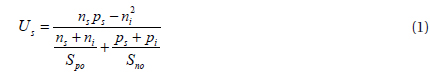
The c-Si-substrate surface constitutes a grievous discontinuity of its crystalline structure. It is well known that a Si atom has four valence electrons and each requires one valence electron from another Si atom to be paired. At the c-Si surface, there are not enough atoms to pair all of the valence electrons, and the unpaired electrons are commonly referred to as “dangling bonds.” Dangling bonds create a large density of surface states (defects) between the conduction and valence bands. Each surface state acts as a recombination center, resulting in a significantly high recombination probability. The surface recombination rate (Us) for a single defect at the surface is given by the following equation [3]:
where ns and ps are the concentrations of the electrons and holes at the surface, respectively; ni and pi represents the intrinsic carrier concentration; and Sno and Spo are the SRV parameters for the electrons and holes, respectively. The SRV parameters can be related to thermal velocity (νth) and surface trap density, as follows:

where Nts is the surfacetrap density, and σn and σp represent the capture cross-sections for the electrons and holes, respectively.
The SRV can be related to Us in the following equation:

where S is the SRV and Δns is the excess carrier density at the surface.
When the semiconductor surface is in the flat-band condition, the excess concentrations of electrons (Δns) and holes (Δps) are equal under illumination; then, we can use Δns to represent the excess carrier concentration at the surface. Note that Δns is constant in the semiconductor from the bulk to the surface, as the energy bands are flat [5]. SRV can also be calculated from the following expression:
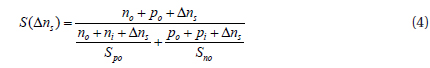
where no and po are the electrons and holes of the equilibrium concentration, respectively. According to the above equation, SRV is a function of parameters, injection level (ratio between changes of the minority carrier concentration and majority carrier concentration, known as “injection level”), and doping concentration. SRV parameters are determined by the trap energy level (Et), trap density (Nts), and capture cross-sections for electrons and holes. SRV is used for quantifying the surface recombination process. In general, it is improved by the following: (i) decreasing the defect states at the interface, leading to a low recombination rate (chemical passivation), and (ii) achieving the reduction of the surface concentration of the minority carriers (field-effect passivation).
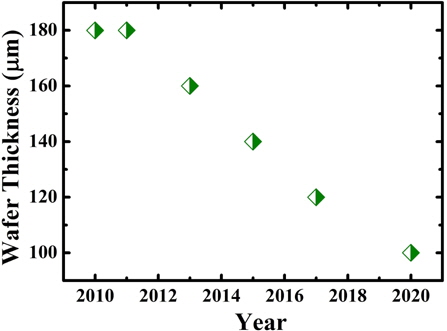
Figure 2 depicts the impact of the chemical and field-effect passivation schemes, reduction of the interface state density (Dit), and field-effect passivation.
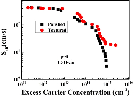
The thermal growth of silicon dioxide (SiO2) is the most effective surface passivation technique for c-Si solar cell. The SiO2 growth formed at a high temperature (>900℃) possesses a low interface-state density (1×10¹⁰/cm2eV) [6,7]. A high temperature, however, degrades the bulk life time and stability of the passivated surface significantly; therefore, this technique is not suitable for low-cost industrial processes [8]. A record-low, effective surface-recombination velocity (Seff) of 4 cm/s was obtained on 1 Ω-cm p-type c-Si wafers by using PECVD SiNx [9-12]. The fieldeffect passivation provided by the positive interface charges, the properties of the captured cross-sections of dominant defects, the adjustable ARC refractive index, and the hydrogen passivation of bulk defects made SiNx a superior passivation layer over the other passivation materials [5,8,13,14].
In 1972, Mandelkorn, et al., introduced the rear-surface passivation of Si solar cells, whereby a homojunction was used to suppress the minority carrier concentration across the full back surface, and this technique has since been referred to as “BSF” [15]. To further improve efficiency, enhanced rear-passivation techniques beyond the simple full area of Al-BSF is a prerequisite prerequisite. In 1989, the first so-called “passivated-emitter and rear cell” (PERC) was fabricated by Blakers et al. [16]. These cells feature a dielectric passivation with locally defined contact openings and a full-area metallization on the rear. Shortly afterward, the same group introduced the “passivated emitter, rear locally diffused” (PERL) cell [17] with thermal SiO2 that gave the lowest SRV and a high-efficiency [18]. In addition to SiNx:H [8,21], atomic-layer deposition (ALD) of Al2O3 gives an SRV at lower temperatures that is similar to that of SiO2 [19,20].
4.3.1 Thermal SiO2
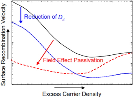
The high-quality interface between thermally grown SiO2 and c-Si contributes significantly to a high efficiency [22,23]. Thermal SiO2 leads to a very low SRV after the annealing process [16,23-26].The hydrogen that is introduced during annealing passivates electronically active defects with defect densities in the region of 1010 cm−2eV−1 [23,27] and fixed charges (Qf) in the range of 1010 cm−2 to 1011 cm−2. In addition, the SiO2/Al stack at the rear side of the cell acts as an excellent reflector for near-band-gap photons and significantly improves the light-trapping properties, thereby also improving the short-circuit current of the cell. A Seff of less than 3 cm/s was achieved by M. Kerr, et al. on FZ wafers [25], and a Seff of less than 20 cm/s was obtained on n-type CZ wafers [28]. The SRV increases with the doping density due the higher presence of their defects at the interface, and this trend is represented in Fig. 3. Zhao, et al. obtained a high-efficiency of 25% with a SiO2-passivation scheme on their PERL cell concept [29-31]. Since oxidation usually takes place at very high temperatures and needs a considerably long time duration, it is not widely used in industrial solar cell mass production in the current time period.
Schultz et al. carried out a wet oxidation process using pyrogenic steam at 800℃ and studied the rear-surface passivation properties on FZ Si [1,32]. The absolute gains of 6% in both Jsc and Voc in a comparison with conventional Al-back BSF cells are due to their high internal reflectance in the long-wave region.
4.3.2 SiOx
To overcome bulk lifetime degradation, a low-temperature SiOx deposition by PECVD has been studied by different groups [33-35] for surface passivation. Another option for the synthesis of SiOx is a chemical oxidation of the Si surface using nitric acid (HNO3). A drawback of this method is that it can only produce a SiOx with a thickness of a few nanometers. In general, the level of passivation induced by a single-layer SiOx synthesized at low temperatures is lower than that obtained by thermal oxidation processes. Mihailetchi et al. successfully fabricated a cell with an ultrathin SiOx layer by soaking the Si wafers in a solution of HNO3 prior to the deposition of SiNx as an ARC for effective boronemitter passivation, whereby the Voc is 627 mV and the efficiency is 18.3% [36].
4.3.3 a-SiNx:H
Over the past decade, PECVD-deposited SiNx has been the dominant surface passivation method for the Si photovoltaic industry [19,37,38]. SiNx is deposited using a SiH4 and NH3 gas mixture at a temperature of approximately 200℃, with the process pressure varying between 0.1 and 1 mbar. In direct PECVD, the process gasses are excited by an alternating electromagnetic field where the wafers form the electrodes. In batch systems, the wafers are loaded into graphite boats acting as electrodes and the wafers are processed in a quartz tube. An alternative approach is the remote PECVD process; in this method, plasma excitation is spatially separated from the wafer. A linear plasma source is used wherein microwaves from an external source are coupled in the process chamber. The wafers are loaded onto carbon-fiber-composite carriers and are moved horizontally through the plasma chamber. Direct and remote PECVD systems have the highest market share in the photovoltaic industry because of their high throughput and low process temperatures. Thefilms contain a relatively large amount of hydrogen (10 at.% to 15 at.%) that mainly originates from the SiH4.
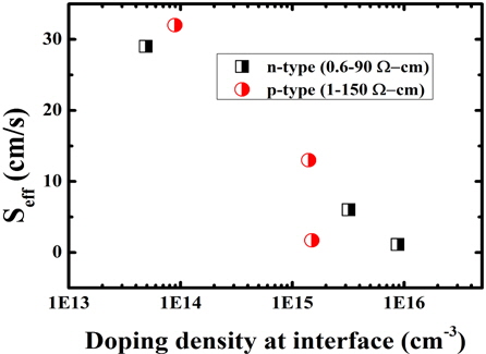
By varying the SiH4 and NH3 compositions, both built-in charges and the surface states can be varied. Here, field-effect passivation is achieved by producing a high concentration of charges in the dielectric that originates from a number of defect states that are formed either at the nitride/c-Si interface or in the bulk of the film. For textured and polished surfaces passivated with SiNx, measured Seff as a function of the excess electron concentration is depicted in Fig. 4.
The SiNx film, with a refractive index (n) of 2, results in optimal antireflection properties. Nitrogen-rich SiNx films where n=2 provide a reasonable-to-high level of passivation. When the nitrogen content is relatively low (i.e., in SixNy, x>y), the high level of passivation is mainly governed by chemical passivation. Alternatively, for a high nitrogen content, the films induce a significant amount of field-effect passivation with fixed charge densities in the region of 1,012 cm−2. The presence of these fixed charges is due to the presence of Si and nitrogen dangling bonds, normally denoted as “K center” and “N center,” respectively [39]. In stoichiometric nitrides (i.e. Si3N4), the K centers (Si atom backbonded with three N atoms) [40,41] can be charged positively [42-44]. This significant positive-charge density leads to a strong inversion layer on the p-type c-Si surfaces, known as the “parasitic” or “inversion-layer shunting effect,” leading to a reduction of the short-circuit current and cell efficiency [45]. SiO2/SiNx stacks are expected to reduce or nullify this detrimental effect [46, 47].
4.3.4 Al2O3
Aluminum oxide (Al2O3) has recently emerged as a passivation layer for n-type c-Si solar cells owing to its excellent field-effect passivation that is associated with the negative fixed charges near the Al2O3/c-Si interface [19,48,49] that proved to be beneficial, especially for boron-emitter passivation, in comparison with SiNx and thermally grown SiO2. An efficiency of 23.9% was obtained by applying Al2O3 layer on the boron emitter [50,51]. Al2O3 films are coated by a plasma-assisted method as well as a thermal-ALD method with a very low deposition rate of < 2 nm/min [19,48,52-55]. After annealing Al2O3 films at moderate temperatures, an outstanding Seff of <5 cm/s was obtained [49,53] on a low-resistive p-type wafer, and < 1 cm/s was obtained on an n-type c-Si wafer (1 Ω-cm to 4 Ω-cm). After the annealing process, the SiO2/Al2O3 stack yields a high level of chemical passivation due to a low interface defect density [56]. Using the SiO2/Al2O3 stack, an excellent efficiency of 21.5% has been obtained; furthermore, the Al2O3 film overcomes the so-called “parasitic shunting” effects that are very common for SiNx-passivated rear passivation [45]. The main disadvantage of ALD for photovoltaic applications is a low deposition rate; however, this disadvantage can be overcome by depositing ultrathin (2 nm to 30 nm) Al2O3 films using ALD and capping them with a thicker SiOx film deposited by PECVD. Another disadvantage is that ALD/Al2O3 film degrades substantially during the firing process; therefore, a capping layer such as SiNx [57] is required. A combination of ALD and PECVD may be a key technology for future industrial, high-efficiency solar cells. The passivation effects of different passivation materials and their industrial compatibilitiesare depicted in Table 1.
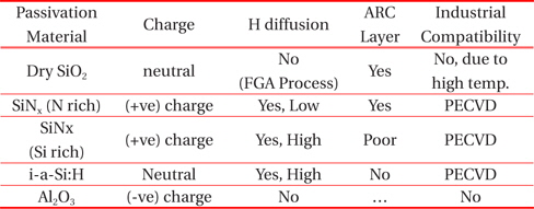
Passivation effects of different passivation materials and their industrial compatibilities.
4.3.5 PECVD-ONO
Thermally grown SiO2 layers provide all of the following major characteristics that are required for a rear passivation for p-type c-Si based PERC solar cells: sound surface passivation, effective rear reflectance, and thermal stability. Unfortunately, thermaloxide growth requires a long (~90 min) high-temperature process that reduces the original carrier lifetime; also, the oxidation process produces a medium throughput. PECVD Si-oxide (SiOx) film may be a possible alternative to SiO2 film due to the benefits of the PECVD process. Stacks of PECVD SiOx/SiNx (or ON) and PECVD SiOx/SiNx/SiOx (or ONO) have been investigated. These stacks resulted in as-deposited Seff values of <700 cm/s (ON) and <240 cm/s (ONO); subsequently, FGA at 425℃ resulted in Seff values of <50 cm/s (ON) and <30 cm/s (ONO) [58,59].
4.3.6 A-Si:H
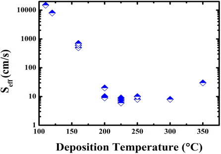
The excellent material properties of the intrinsic hydrogenated amorphous silicon (i-a-Si:H) has attracted considerable attention in the field of heterojunction solar cells since it replaces the high-temperature dopant diffusion process of the intrinsic a- Si:H films at a low temperature.
Figure 5 represents the measured SRV of PECVD-deposited i-a-Si:H films as a function of the deposition temperature [60]. A-Si:H films are usually deposited by conventional PECVD at approximately 225℃ and contain a large amount of hydrogen (>10 at.%) [60]. This hydrogen content effectively passivates the c-Si/ a-Si:H interface, resulting in a low interface-state density. The passivation principle of intrinsic a-Si:H is based on hydrogenrelated chemical passivation. Using intrinsic a-Si:H, excellent passivation properties with Seff that are as low as 2 cm/s were obtained [61-64] with a high Voc of >700 mV. Sanyo achieved a world-first high efficiency of 25.56% [65] on a-Si:H/c-Si heterojunction solar cells; using device modeling, the efficiency is reported to be 26.61% [66]. The parasitic absorption effects and the lack of thermal stability during a high-temperature process are the major limitations of applying a-Si:H film to be applied as a passivation layer; therefore, a-Si:H films cannot be applied in the production of standard, screen-printed solar cells. The variety of surface passivation methods that have been used in different kinds of c-Si solar cells are depicted in Table 2.
[Table 2.] Surface passivation methods of c-Si solar cell.

Surface passivation methods of c-Si solar cell.
One way to achieve a high efficiency that is well above 20% at a reduced cost relies on the use of thinner wafers. Surface passivation is the most vital matter here, and passivation material is critical for the production of high-efficiency c-Si solar cells.
Due to the low growth rate or deposition rate of passivation, the extremely high-temperature process for the growth of SiO2 has seldom been adopted as a passivation scheme for highefficiency c-Si solar cells. Recently, even though low surface recombination velocities were achieved using SiNx that had been deposited by PECVD, the high density of the fixed positive charges within the SiNx layer induced parasitic shunting, thereby reducing the short-circuit current density; furthermore, it was also recently shown that, for boron emitters, ALD/Al2O3 (with a capping layer deposited by PECVD) provides an outstanding level of surface passivation, which can be attributed to its extremely high, negative fixed-charge density and low interface-state densities.

![Predicted trend for wafer thickness. Reproduced with permission from [2], International Technology Roadmap for Photovoltaic, Fifth Edition, March 2014. Permission granted. Copyright ⓒ ITRPV 2014 (www.itrpv.net).](http://oak.go.kr/repository/journal/17508/E1TEAO_2015_v16n5_227_f001.jpg)


![Impact of the two passivation schemes, reduction of Dit (blue curve), and field-effect passivation (dashed). Reproduced with permission from [4], S.W. Glunz, High-efficiency of crystalline silicon solar cells; Advances in Optoelectronics, Vol 2007, Article ID 97370, DOI: http://dx.doi.org/10.1155/2007/97370. Permission granted. Copyright ⓒ2007 S. W. Glunz.](http://oak.go.kr/repository/journal/17508/E1TEAO_2015_v16n5_227_f002.jpg)
![Effective surface recombination velocity of both phosphorusdoped (n-type) and boron-doped (p-type) bases as a function of the doping density. Data from [25], Mark J Kerr and Andres Cuevas, Very low bulk and surface recombination in oxidized silicon wafers, Semicond. Sci. Technol. 17 (2002) 35. Permission granted. Copyright ⓒ IOP Publishing 2010.](http://oak.go.kr/repository/journal/17508/E1TEAO_2015_v16n5_227_f003.jpg)
![Measured surface recombination velocity as a function of the excess electron concentration for both textured and polished surfaces passivated with SiNx. From [9], T. Lauinger et al. Record low surface recombination velocities on 1 Ω.□cm p-silicon using remote plasma silicon nitride passivation, Appl. Phys. Lett. 68, (1996) 1232. Permission granted. License number 3674270659162. Copyright ⓒ 1996 American Institute of Physics.](http://oak.go.kr/repository/journal/17508/E1TEAO_2015_v16n5_227_f004.jpg)

![Effective surface recombination velocity as a function of the PECVD i-a-Si:H deposition temperature. FZ p-type c-Si wafers were passivated by PECVD a-Si:H ?lms deposited at different temperatures. Data from [60], M. Schaper et. al.20.1% efficient crystalline silicon solar cell with amorphous silicon rear surface passivation, Prog. Photovolt: Res. Appl. 13 (2005) 381. Permission granted. License number 3674261095667. Copyright ⓒ 2005 John Wiley & Sons, Ltd.](http://oak.go.kr/repository/journal/17508/E1TEAO_2015_v16n5_227_f005.jpg)