A charge-trap flash (CTF) thin film transistor (TFT) memory is proposed at a low-temperature process (≤ 450℃). The memory cell consists of a sputtered oxide-nitride-oxide (ONO) gate dielectric and Schottky barrier (SB) source/drain (S/D) junctions using nickel silicide. These components enable the ultra-low-temperature process to be successfully achieved with the ONO gate stacks that have a substrate temperature of room temperature and S/D junctions that have an annealing temperature of 200℃. The silicidation process was optimized by measuring the electrical characteristics of the Ni-silicided Schottky diodes. As a result, the Ion/Ioff current ratio is about 1.4×10⁵ and the subthreshold swing and field effect mobility are 0.42 V/dec and 14 cm2/V·s at a drain voltage of −1 V, respectively.
Low-temperature polycrystalline silicon (LTPS) thin film transistors (TFTs) have been widely used for applications such as switches in active-matrix liquid crystal displays (AMLCDs) and active-matrix organic light emitting diodes (AMOLED) because of their high field effect carrier mobility, high driving current and uniformity of polycrystalline silicon (poly-Si) compared to conventional amorphous silicon (a-Si) [1,2]. In addition, further improvement in the performance of the poly-Si TFT can enable the integration of various functional devices, such as the memory and controller, on a glass panel to achieve system-on-panel (SOP) display. The low-power consumption is the highest priority requirement for various SOP applications [3]. However, the increase in power consumption and degradation of the panel’s brightness still persists in SOP applications. However, the increase in power consumption and degradation of the panel’s brightness still persist in SOP applications.
Recently, in order to completely solve these problems, non-volatile memories (NVMs) have been embedded as the memories of flat panel display pixels due to their ability to store images in electric devices and reduce the degradation in the brightness of the panel [4]. For LTPS NVMs, an oxide-nitride-oxide (ONO) stack structure functioned as the blocking-charge trapping-tunneling layer.
However, ultra-thin ONO film formation at a low temperature has not been investigated. On the other hand, innovations in low-temperature fabrication have been proposed in flash memory with Schottky barrier (SB) source/drain (S/D). The SB S/D has numerous advantages; it is a simple low-temperature process (less than 500℃), and offers low parasitic S/D resistance and strong short-channel-effect immunity. Furthermore, it has inherent physical scalability to sub-100-nm gate lengths [5-8].
In this work, we present the low-temperature TFT charge-trap flash memory with sputtered ONO gate dielectric and SB S/D junction.
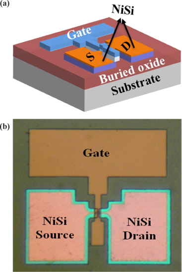
Figure 1 shows the schematic structure of an LTPS NVM cell with sputtered ONO and SB S/D using Ni silicide. First, we used a furnace system to grow 300-nm-thick thermal oxide on the p-Si wafers for the insulting layer. Then, a 100-nm-thick a-Si layer was deposited on an SiO2/p-Si substrate using low-pressure chemical-vapor deposition, by the dissociation of SiH4 gas. Subsequently, solid-phase crystallization (SPC) was performed for 24 hours in ambient N2 by using an annealing furnace. After standard RCA cleaning, the active region with a 20 μm channel length of poly-Si SB-TFTs was defined by photolithography and plasma reactive ion etching (RIE) processes. In order to form the metallic junctions at the S/D regions, we deposited a 30-nm-thick Ni film by using an e-beam evaporator.
Subsequently, to form the Ni-silicide source/drain, rapid thermal annealing (RTA) was performed at 300℃ for 30 sec in ambient N2. Subsequently, an ONO layer with a thickness of 5/10/50 nm was deposited in-situ by using DC-magnetron sputtering. The thicknesses of the ONO stacks were confirmed to be 5/10/10 nm by spectroscopic ellipsometry. Using the e-beam evaporator, the following deposition of the 150-nm-thick Al film for the gate electrodes was conducted. Then, the gate electrode was patterned with a channel width of 20 μm.
Finally, the fabricated devices, as shown in Fig. 1(b), were annealed in 2% diluted ambient hydrogen (H2/N2) at 450℃ for 30 minutes to improve the electrical characteristics. All electrical measurements were performed at room temperature, and the channel width/length (W/L) of the fabricated devices were 20/20 μm.
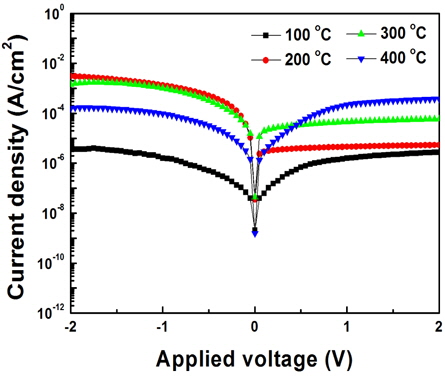
In order to determine the annealing temperature condition of Ni-silicide S/D, the junction current density and the applied voltage (I-V curves) was investigated for different annealing temperatures from 100℃ to 400℃ at the n-type Si substrate, as shown in Fig. 2.
In order to form the junction diode with Schottky barrier, a 30-nm-thick Ni film was deposited by using an e-beam evaporator at room temperature. Subsequently, the silicidation annealing process was performed from 100℃ to 400℃ for 30 sec in ambient N2.
The results indicate that only the Ni-silicide/n-Si contact annealed at 300℃ has the highest electron barrier height (or the lowest hole barrier height), while the different annealed conditions at 100, 200 and 400℃ have significantly higher leakage currents at a reverse bias. Based on these data, we determined the optimal annealing temperature to be 300℃ because of the lowest reverse bias leakage current, and the best rectifying property with a near unity ideality factor. The Schottky barrier height value for electrons was deduced as 0.685 eV from linear fittings based on the thermal emission model [9].
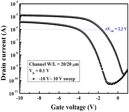
Based on the optimized condition of Ni-silicide S/D, Figure 3 shows the drain current-gate voltage (ID-VG) and drain current-drain voltage (ID-VD) curves for the fabricated TFTs with sputtered ONO gate dielectric and Ni silicided S/D junctions.
The Ion/Ioff current ratio is about 1.4×10⁵ and the subthreshold swing (SS) and field effect mobility (μFE) are 0.42 V/dec and 14 cm2/V·s at a drain voltage of −1 V, respectively, as shown in Fig. 3(a). Figure 2(b) shows the drain current-drain voltage (ID-VD) curves as a function of gate voltage applied from 0 V to −7 V with −1 V steps. The behavior is typical of field effect TFTs showing partial saturation effects at high VD. These results indicate that the fabricated device has superior performance, such as the high on current, high μFE, small SS.
Finally, Figure 5 shows the memory window versus the gate voltages for the TFT. The gate biases were varied from −10 to 10 V during the ID-VG sweep. The memory window was found to be 2.2 V. This result indicates that many charges could be trapped in the Si3N4 trapping layer (10 nm-thick) deposited by the ONO layer.
This research proposes a charge-trap flash TFT structure that has a sputtered ONO gate dielectric and Ni-silicide SB S/D junctions at a low-temperature. As a result, the Ion/Ioff current ratio is about 1.4×10⁵, and the SS and μFE are 0.42 V/dec and 14 cm2/V·s at a drain voltage of −1 V, respectively. A memory window of 2.2 V was obtained. These LPTS TFTs memories with sputtered ONO films and Ni-silicided S/D junctions are very useful for fabrication of the small-dimension system on the panel.