We have reported about bipolar resistive switching effect on Poly[2-methoxy-5-(2-ethylhexyloxy)-1,4-phenylenevinylene]:Graphene oxide composite films, which are sandwiched between aluminum and indium tin oxide electrodes. In this case, I-V sweep curve showed a hysteretic behavior, which varied according to the polarity of the applied voltage bias. The device exhibited excellent switching characteristics, with the ON/OFF ratio being approximately two orders in magnitude. The device had good endurance (105 cycles without degradation) and long retention time (5 × 10³ s) at room temperature. The bistable switching behavior varied according to the trapping and de-trapping of charges on GO sites; the carrier transport was described using the space-charge-limited current (SCLC) model.
In past few decades, many research studies have been conducted on organic-based electronic devices [1,2]. Organic bistable memory devices (OBDs) have attracted tremendous attention as they could be used as flexible nonvolatile memory devices in the near future. The OBDs, which consist of conducting polymers and inorganic nanoparticle hybrid layers, have several advantageous properties, such as good reproducibility, high device performance, and versatile functionality. A spincoating fabrication process is used to construct these OBDs in a cost-effective manner [3]. Subsequently, graphene sheets are incorporated in the organic materials, which act as charging and discharging media. Therefore, OBDs could be potentially used for constructing hybrid nanocomposites, which are used in non-volatile memory devices [4]. Recently, few studies have reported that polymers, such as poly (Nvinylcarbazole) [5], triphenylamine-based polyazomethine (TPAPAM) [6], polyimide [7] etc. can be combined with graphene to prepare composites for use in non-volatile memory devices. While fabricating such devices, it is not necessary to precisely maintain vacuum and temperature. Thus, such composites can be easily constructed with a simple fabrication process.
Among the various organic polymers with optoelectronic applications, Poly[2-methoxy-5-(2-ethylhexyloxy)-1,4-phenylenevinylene] (MeH-PPV) is the most studied polymer in the past few decades; However, very few reports have described about its non-volatile resistive memory. Li
To prepare the composite film, graphene oxide (GO) flakes and MeH-PPV were purchased from graphene supermarket (USA) and Sigma Aldrich (USA), respectively. Graphene oxide (1 mg) was dispersed in 10 ml of toluene; the suspension was ultrasonicated for 2 h. Then, MeH-PPV (5 mg) was mixed directly with the above solution. Thereafter, we ultrasonicated the solution for 30 min. Thus, we obtained the final solution, which was used to prepare the composite film. Before coating the film, the ITO substrate was cleaned by a standard cleaning procedure. Then, we deposited the sol dropwise on the substrate at a constant rotating speed of 2,500 rpm for 60 s. An aluminum film of 100 nm thickness was thermally evaporated using shadow mask to ensure top metal contact. Thereafter, these films were characterized using scanning electron microscopy (SEM) and energy dispersive spectrometry (EDAX) techniques. Electrical measurements were recorded using Keithley 4200DC parameter analyzer.
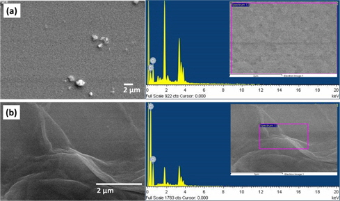
Figure 1(a) and (b) display the SEM images of pure MeH-PPV and MeH-PPV:GO composite film, which are deposited on the ITO substrate. The polymer and ITO substrates give rise to low intensity carbon and oxygen peaks in the EDAX spectrum of pure MeH-PPV film, while the presence of GO in the composite films gave rise to high intensity peaks (inset Fig. in 1(a) and (b)).
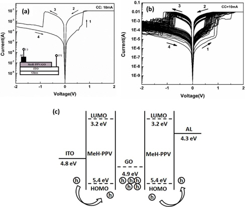
Figure 2(a) and (b) display the single and 130 consecutive
The resistive switching mechanism of Al/MeH-PPV: GO/ITO device may be attributed to the charges captured by the GO flakes. The GO flakes act as traps, capturing carriers that are injected from the electrode. Thus, they generate a strong local internal field inside the organic layer. As a result, this device changes its conductance upon bias [10]. As shown in the energy level band diagram (Fig. 2(c)) [11,12], the highest occupied molecular orbital (HOMO) and the lowest unoccupied molecular orbital (LUMO) of MeH-PPV occur at 5.4 and 3.2 eV, respectively. In the active layer of MeH-PPV:GO, the energy difference between the work function of Al and LUMO of MeH-PPV (1.1 eV) is higher than the energy difference between the work function of ITO and HOMO of MeH-PPV (0.6 eV). Owing to this energy difference in the work functions, the injection of holes is favored from the ITO electrodes into the HOMO of MeH-PPV layer. Hence, during the positive voltage sweep, the holes from the ITO electrode are injected into the composite layer, while the injected charge carriers sufficiently fill the trapping centers in GO layer. Therefore, the interfacial resistance of GO is reduced, and the ON state of the device is attained. In the negative sweep, the trapped holes are released from the charge trapping centers. Thus, the OFF state of the device is attained [13]. Under the effect of reverse bias, the captured holes easily release from the shallow traps (0.5 eV) formed between GO and MeH-PPV. Thus, these shallow traps exhibit bipolar resistive switching effect.
We comprehensively studied the conduction and switching mechanisms of the memory device using the
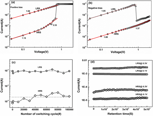
To evaluate the resistive switching stability and the performance window of this novel device, we determined the endurance and retention properties of the device in room temperature at a readout voltage of 0.1 V (Fig. 3(c) and (d)). As shown in Fig. 3(c), the repeated switching process was tested up to 105 cycles using a pulse generator in the ‘burst mode’. There was no noticeable fluctuation in resistance of the ON state. However, in the OFF state, there were slight fluctuations in the resistance as the trapped charges were not erased completely. Moreover, in both HRS and LRS, the resistance varied with time under a stress bias of 0.1 V and 0.3 V, respectively (Fig. 3(d)). Thus, both the resistance states can be retained, regardless of the expended time. Based on these results, we conclude that MeH-PPV:GO film exhibits a bistable resistive switching behavior, which is reversible and steady. Therefore, it can be conveniently used in flexible nonvolatile memory applications.
Bistable memory devices can be fabricated using MeH-PPV:GO composite film, which is sandwiched between Al and ITO electrodes. The probable switching mechanism of the device depends on the hole trapping in GO flakes. The devices have an impressive ON/OFF current ratio, which is approximately two orders in magnitude. These devices have long retention time of up to 5 × 10³ s. They also exhibit superior endurance of up to 105 cycles and require low energy for performing the write and read operations of memory. Compared to the multilayer structure of conventional devices, the fabrication approach of these novel devices involves a single step process, which is more advantageous. In these novel devices, the memory is improved due to the use of polymeric materials, which are prepared by a simple process method. These novel devices are of low cost, so they can be used in next generation non-volatile memory applications.