We investigated the formation of a nanopyramidal structure and fabricated nanotextured Si solar cells using an Ag metal-assisted chemical etching process. The nanopyramidal structure was formed on a Si flat surface and the nanotexturing process was performed on the p-type microtextured Si surface. The nanostructural formation shows a transition from nanopits and nanopores to nanowires with etching time. The nanotextured surfaces also showed the photoluminescence spectra with an enhanced intensity in the wavelength range of 1,100~1,250 nm. The photoreflectance of the nanotextured Si solar cells was strongly reduced in the wavelength range of 337~596 nm. However, the quantum efficiency is decreased in the nanotextured samples due to the increased nanosurface recombination. The nanotexturing process provides a better p-n junction impedance of the nanotextured cells, resulting in an enhanced shunt resistance and fill factor which in turn renders the possibility of the increased conversion efficiency.
The surface texturization of Si solar cells has an important role in reducing the photoreflectance (PR) losses and increasing the photoabsorption of the cells to improve the overall electrical characteristics such as short-circuit current (Isc), open-circuit voltage (Voc), and conversion efficiency [1-3]. However, the textured surfaces are also inefficient in reducing the PR to less than 10%. Therefore, SiNx as an anti-reflection coating (ARC) layer has been deposited on solar cells to reduce the PR and act as a surface passivation layer; however, it exhibits narrow acceptance of the incident light due to the destructive interference of the reflected light [4]. Further, several nanostructures have been implemented in order to improve the light absorption of solar cells by wave diffraction effect, which can efficiently transmit light into the Si solar cells and enhance the shunt resistance of pn junction [5-7]. Among these nanostructures, nanotextured black Si solar cells have attracted considerable attention due to their low reflectivity over a wide spectral range that improves conversion efficiency to over 18% [8-10].
Several methods have been developed for the nanotexturing of the Si solar cell surface including laser texturing, reactive ion etching (RIE), nanoimprint lithography, and metal assisted chemical etching (MACE) [11-15]. Due to the high cost and process complexity of RIE, laser texturization, and nanoimprint lithography, their applications in Si solar cells are limited. Therefore, metal assisted chemical etching has been investigated to obtain nanotextured Si solar cells due to its low cost and simple fabrication process over a large surface area [16]. It has been found that the nanotextured Si solar cells prepared by MACE process via HF and AgNO3 aqueous solution can reduce the reflection to below 2% [17]. However, nanotextured Si solar cells prepared using the MACE process suffer from surface recombination and Auger recombination due to their large surface area. This is attributed by the non-uniform heavy etching which limits the short circuit current and the conversion efficiency. Therefore, it is necessary to control the MACE process in order to obtain a uniform shallow nanotextured Si surface that can reduce the surface recombination and increase the cell performance.
In this work, we formulated the nanopyramidal structure from a flat Si (100) wafer and fabricated nanotextured surfaces on microtextured single crystalline Si solar cells using metal-assisted chemical etching. The nanotexturing process is controlled to form shallow nanopores and the PR of the nanotextured Si is significantly reduced in the UV-VIS region of the solar spectrum. The quantum efficiency is also reduced from the nanotextured surface. However, photoluminescence spectra are enhanced and the overall conversion efficiency of the fabricated nanotextured Si solar cells is also improved compared to the reference cell.
The micropyramid and nanopyramid surfaces on Si solar cells were formed by alkali solutions of KOH and NaOH, respectively. P-type boron-doped single crystalline 6-in Si wafers with a specific resistance of 0.5~3 Ω cm and a thickness of 200±5 μm were used for the fabrication of the shallow nanotextured solar cells. The detail process flows are illustrated in Fig. 1. A microtexturing process for micropyramid formation was carried out in a KOH-isopropyl alcohol (IPA) solution at a temperature 80℃ for 45 min followed by saw damage removal. In order to remove the K contaminants, the textured wafers were cleaned in HCl:H2O2:H2O mixture at 80℃ for 10 min and the wafer surfaces were then H-terminated by dilute HF and rinsed with sufficient distilled (DI) water. However, the nanotexturing process for nanopyramid formation was carried out in 1% NaOH solution at a temperature of 80℃ for 10 min followed by saw damage removal. The samples were sufficiently rinsed with DI water and treated with 6% HCl for 15 min in order to remove the Na residual. After the Na residual removal, the samples were treated with 5% HF to remove the surface oxide. Finally, a RCA-2 cleaning process was carried out by HCl:H2O2:H2O (1:1:6 vol%) for 10 min and the formed oxide was further removed by 5% HF. The samples were then sufficiently rinsed by DI water and also dried by a N2 gun.
Further nanotexturing processes on the micropyramid and nanopyramid surfaces were carried out using a one-step MACE process involving a HF:AgNO3 solution. For the etching on the microtextured surface, the amount of AgNO3 was 0.005 M, the amount of HF was 0.014 M, and the etching time was varied. It is important to note that a very low concentration of HF and AgNO3 solution was used and the cells were etched for a short time because high concentration and long etching time caused over-etching of the microtextured surface which increases the surface recombination [18]. The nanotexturing process on the nanopyramid was performed with the high concentration of HF:AgNO3 (5:0.01 M) solution for an etching time of 10 sec. After the nanotexturization process, the Ag residuals remaining on the solar cell surfaces were removed by dipping in concentrated HNO3 acid for 3 min and sufficiently rinsing with DI water. The wafers were then treated with a mixture of HCl:H2SO4:H2O at a volume ratio of 1:1:2 at 70℃ for 10 min in order to remove the HF contaminants remaining after the nanotexturing process. The oxide formed by this process was removed with 10% HF for 1 min.
The emitter layer was formed using a tube furnace diffusion process and POCl3 liquid was used as the doping source.
The doping process was carried out by two steps of the predeposition and the drive-in process under O2 and N2 carrier gases, respectively, in order to obtain a sheet resistance of 55 Ω/sq. During the pre-deposition process that carried out for 10 min at 750℃, a P2O5 layer was formed and worked as a phosphorous dopant source on the Si solar cell surface. Phosphorous was diffused into the solar cell using the drive-in process at 820℃ for 10 min and phosphor-silicate glass (PSG) was formed on the surface. This PSG layer was removed with a 10% HF solution. After the removal of the PSG layer, an 80 nm thick SiNx layer as an ARC layer was deposited under SiH4:NH3:Ar gas for 10 min using plasma enhanced chemical vapor deposition (PECVD). The front silver pattern contact and aluminum back surface field were formed using a screen-printing technique and dried at 200℃. A co-firing process was then carried out in a belt IR furnace at 400~850℃. Finally, the edge isolation process was performed to prevent current leakage.
The fabricated solar cells were characterized using various measurement tools including a field emission scanning electron microscope (FESEM) to study the surface morphology of the cells. The PRs of the textured wafers and the fabricated solar cells were measured using a UV-VIS-NIR spectrophotometer. The p-n junction of the solar cells and Ohmic contact properties were characterized from photoluminescence and electroluminescence images (McScience Co. K3300). The quantum efficiency was measured (ICPE system Co. QEX7) with a Xenon arc lamp that converts the incident photons to currents.
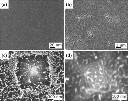
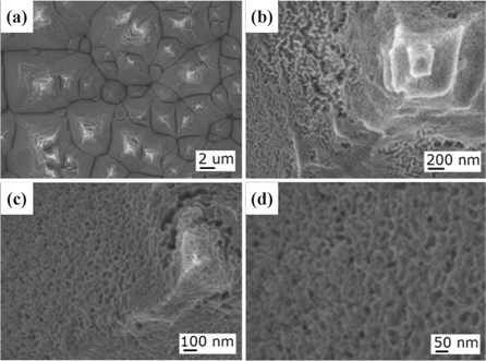
Figure 2 shows the FESEM images of the nanotextured nanopyramidal structure with the high concentration of HF:AgNO3 (5:0.01 M) solution for an etching time of 10 sec. An Ag MACE process was carried out on the nanopyramidal surface of flat wafer. Ag nanodendrites covered the flat surface and showed the local contact with Si where the contact potential is derived from the etching process. The surface showed the formation of the nanoporous structure as various nanopits and pyramids with the dimension range of 1~3 μm. The nanoscale-sized pyramids are observed on the nanoporous surface as shown in Fig. 2(d). This is applicable to the formation of the nanotextured surface on the microtextured wafer.
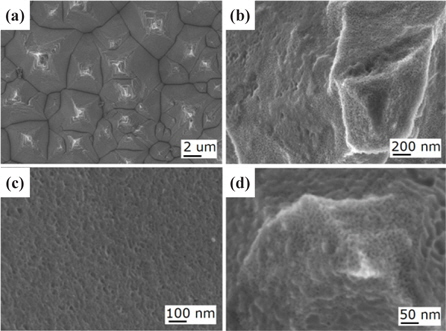
Figure 3 shows FESEM images of the nanotextured Si solar cell on the microtextured wafers etched using the concentration of HF:AgNO3 (0.14:0.005 M) solution with the etching time of 30 sec. The diluted etching solution provides the uniformly nanotextured hillsides with nanopits on micropyramids indicating very shallow etching with a low roughness of the cells for 30 sec.
Figure 4 shows FESEM images of the same nanotextured Si solar cell with the etching time of 1 min. The micropyramids were nanoetched and formed roughened nanosurfaces, which were slightly damaged on the top area due to the increased etching process from the non-uniform formation of Ag dendrites at the top areas.
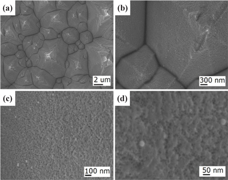
Figure 5 shows the FESEM images of the same nanotextured Si solar cell with the etching time of 3 min. This sample showed severe damages on the top area of the micropyramids due to the over-etching process resulting in the formation of low dense ultra-small nanospikes similar to nanostructures. The Ag metal-assisted nanotexturing process shows the dark gray surfaces of Si wafers visible to the naked eye. This indicates that a surface morphology can be transited from nanopits to nanospikes when the etching time is increased from 30 sec to 3 min.
The nanotexturing mechanism of the MACE process has been described in our previous article [18]. The nanotexturing process is regulated by the cathodic and anodic reaction between the etchant solution and Si. The etching rate is increased with high concentration of HF:AgNO3 solution. The catalytic surface reaction between Ag nanodots and the Si surface can occur due to the surface plasmon effect. The high concentration of HF:AgNO3 solution dissolves the Si micropyramidal surface rapidly, even for a small etching time of 10 sec. When the etching time is increased, the dissolution of Si is also increased, and this destroys the micropyramids of the solar cell surfaces. However, the nanotexturing process with the low concentration of the HF:AgNO3 solution indicates low etching rate. At the etching time of 30 sec, the formed nanopits reveal the initiation of the nanotexturing process by the reduction of Ag ions at the Ag/Si interface, resulting in the formation of SiO2 which is dissolved by HF. For the 30 sec etching time, the area between the top and the bottom of the micropyramids is uniformly etched due to the formation of nanopits. At the etching time of 1 min, nanopores are formed due to the confinement of the Ag nanoparticles in the nanopits during the etching process. When the etching time increases, the rate of the cathodic and anodic reaction also increases, which accelerates the hole injection in the Si, while a larger number of the Ag nanoparticles attach to the top of the micropyramids than the valley parts. These Ag nanoparticles further sink more vertically into the Si and over-etch the top of the micropyramids causing non-uniform etching. Therefore, the nanotexturing process can be optimized to a relatively short time and high concentration for a nanopyramidal surface but to a relatively long time and low concentration for a micropyramidal surface. The nanopores formed on the microtextured surfaces of the Si solar cells have the tendency to act as an anti-reflection layer to improve the conversion efficiency [19-21]
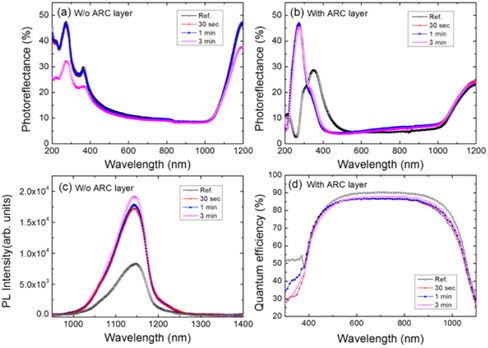
Figure 6 shows the photo-reflectance (PR) properties of the nanotextured cell without and with the SiNx layer, the photoluminescence (PL) by YAG laser excitation, and the internal quantum efficiency (QE) measured under a Xenon arc lamp for the conversion of incident photons to currents. Figure 6(a) shows the PR of the Ref. and nanotextured Si solar cell samples etched for 30 sec, 1 min, and 3 min without an ARC layer. The PR of the nanotextured samples etched for 30 sec and 1 min is slightly reduced in the UV/VIS region of a wavelength range of 390~700 nm and is reduced further in the same region for the 3 min etched sample. The PR of the fabricated nanotextured Si solar cells is significantly reduced in the wavelength ranging from 337 to 596 nm with an 80 nm thick SiNx anti-reflection coating layer as shown in Fig. 6(b). The cell nanotextured for 3 min shows the lowest 4% PR in the visible wavelength range of 451~596 nm. The PR of the nanotextured solar cells in the VIS/IR region of the solar spectrum of the wavelength range of 600~1,200 nm is increased more than that of the Ref. The nanotextured cell etched for 3 min has comparatively smaller PR than the cells etched for 30 sec and 1 min, which indicates that a long etching time is better to reduce the PR of Si solar cells. Figure 6(c) shows the PL spectral peak at 1,142 nm of the Si band gap energy region. The nanotextured samples on the microtextured wafers show the enhanced intensities compared to the microtextured Ref. sample. The nanosurface enhances the light extraction from the radiative recombination process by optical pumping. Figure 6(d) shows the internal QEs of the nanotextured and Ref. cells. The microtextured Ref. sample shows a QE of 90.4% and the nanotextured cells etched for 30 sec, 1 min, and 3 min show QEs of about 86.7%, 86.8%, and 88%, respectively.
The reduced PR of the nanotextured Si solar cells in the UV/VIS region of the wavelength of 337~596 nm ensures the nanotexturing effect by the MACE process. The reflectance of the nano/micro-textured solar cells is especially suppressed in the wavelength range of 400~600 nm, which implies that the nanotextured surface with dense nanopores can act as an ARC layer to improve the light absorption by confining the incident light [22]. The enhanced PL extraction from the nanosurface indicates that the Si nanopores increase the surface area and the corresponding nanosurface recombination. However, the nanosurface-related dangling bonds decrease the internal QE and short circuit current [23]. Furthermore, the absorption of short-wavelength photons due to the nanoporous Si surface causes poor blue response due to the high surface recombination [24,25]. Although the nanotextured cells increase surface and Auger recombination, the photogenerated carriers near the Si bandgap contribute to the enhanced light extraction. This indicates that the radiative photogeneration can enhance p-n junction property.
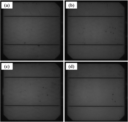
Figure 7 shows the photographic PL images of the Ref. and the nanotextured Si solar cells etched for 30 sec, 1 min, and 3 min. The PL image of the Ref. cell is darker than the nanotextured Si solar cells. The brightness of the nanotextured cells is slightly increased when increasing etching time. Several black spots can also be observed in the PL images where no light absorption or emission occurs.
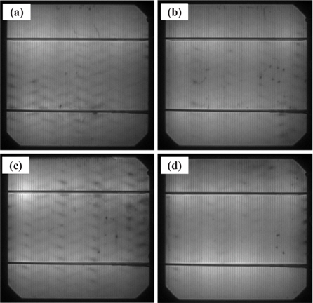
Figure 8 shows the photographic EL images of the Ref. and the nanotextured Si solar cells etched for 30 sec, 1 min, and 3 min. The EL images are bright along the bus bars. The nanotextured cells are brighter than the Ref. cell, which indicates the better Ohmic or shunt property of the p-n junction. Furthermore, the overall brightness in the EL image of the cell etched for 3 min is greater than that of the other cells. Several black spots can also be observed in the EL images which are correlated to the shunt resistance problem.
The enhanced PL and EL in the nanotextured Si solar cells indicate that the electron-hole recombination becomes radiative as shown in the PL emission spectra. The light extraction from the nanosurface can be enhanced due to the reduced wave optical impedance [26]. The wave diffraction from the nanosurfaces can form the delocalized carrier distribution in the depletion layer of the p-n junction. However, the dangling bonds related to the nonradiative recombination from the nanosurfaces can suppress the light emission, which is related to the conversion efficiency [27]. Therefore, the nanotextured surfaces of the Si solar cells show the trade-off relation between the surface non-radiative recombination and the nanostructural light extraction. The improved EL emission by introducing the nanotexturing process is the reverse process of the photovoltaic effect and is reflected in the conversion efficiency of Si solar cells.
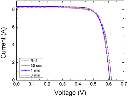
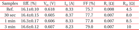
The current-voltage characteristics of the fabricated Ref. and nanotextured cells measured using a solar simulator under the conditions of 100 mW/cm2 and AM 1.5 irradiation at 25℃ are shown in Fig. 9 and summarized in Table 1. The conversion efficiency of the Ref. cell is 16.2% with the fill factor of FF= 75.7%, the open circuit voltage of Voc= 0.618 V, the short circuit current of Isc= 8.33 A, the series resistance of Rs=8 mΩ, and the shunt resistance of Rsh=4.5 Ω. The nanotextured cell with the etching time of 30 sec showed the efficiency of 16.5% with FF=77.7%, Voc =0.605 V, Isc=8.37 A, Rs=7 mΩ, and Rsh=8 Ω. Similarly, the conversion efficiency of the cell etched for 1 min is 16.4% with FF=77.8%, Voc =0.606 V, Isc=8.33 A, Rs=7 mΩ, and Rsh=8.5 Ω. For 3 min-etching time, the nanotextured cell showed the highest conversion efficiency of 16.6% with FF=79%, Voc=0.607 V, Isc=8.23 A, Rs=7 mΩ, and Rsh=10 Ω. The above results reveal that the FF and conversion efficiency of the nanotextured Si solar cells are greater than those of the Ref. cell.
I-V characteristics of the Ref. and shallow nanotextured Si solar cell. The overall conversion efficiency of the shallow nanotextured Si solar cells is improved compared to the Ref. cell.
The overall conversion efficiency of the nanotextured Si solar cells is improved and, especially, the fill factors are strongly improved with enhanced shunt resistances. This electrical behavior can be assumed to be the change of the depletion capacitance with alternating bias, which gives direct evidence of charge mobility [28]. Similarly, the change of optical biasing from ray optics to wave optics can influence the capacitance in the depletion region and the optical forward bias can be reduced in the photovoltaic process. The photoelectric effect can be analyzed by the photocurrent measurement [29]. The wavelength dependent effect of the external quantum efficiency on the photovoltaic property shows similar spectral behavior to that of the photoconductance measured by photoconductive atomic force microscopy [30]. Therefore, the nanotextured cells could not improve the short circuit current and open circuit voltage due to the poor blue response and large surface recombination, but they can be stabilized by reducing the optically induced forward bias in the p-n junction.
A nanotexturing process was performed on the flat surface of a Si wafer and further applied to the microtextured surfaces of 6-in Si solar cell wafers using a MACE process of HF/AgNO3 solutions in order to obtain multi-scale textured surface. The nanotexturing process on the flat wafer showed the nanopyramidal structures, while the nanotexturing process on the microtextured wafer showed a nanosurface hillside of micropyramids. The transition from nanopits to interconnected nanopores was formed by increasing the etching time from 30 sec to 3 min. The blue responses in the QE of the nanotextured cells etched for 30 sec and 1 min were enhanced, and the cell nanotextured for 3 min showed improved QE in the VIS/IR region. The nanotextured cell showed higher conversion efficiencies than those of the Ref. cell. However, the reduced Isc and Voc suggest that surface recombination should be reduced by a better passivation for the nanotextured Si solar cells. In conclusion, the nanotexturing process is useful for achieving higher conversion efficiency and enhancing the shunt property with a high fill factor in the Si solar cell with the reservation of the strong surface passivation on the nanosurface.