Face-to-face (F2F) bonding in three-dimensional integrated circuits (3D ICs), compared with other bonding styles, is closer to commercialization because of its benefits in terms of density, yield, and cost. However, despite the benefits that F2F bonding expect to provide, it’s physical nature has not been studied thoroughly. In this study, we, for the first time, extract cross-die (inter-die) parasitic elements from F2F bonds on the full-chip scale and compare them with the intra-die elements. This allows us to demonstrate the significant impact of field sharing across dies in F2F bonding on full-chip noise and critical path delay values. The baseline method used is the die-by-die method, where the parasitic elements of individual dies are extracted separately and the cross-die parasitic elements are ignored. Compared with this inaccurate method, which was the only method available until now, our first-of-its-kind holistic method corrects the delay error by 25.48% and the noise error by 175%.
Face-to-face (F2F) bonding is a bonding style in threedimensional integrated circuits (3D ICs) where two dies are bonded on their top-metal surfaces. Thus far, many researchers have reported its advantages [1]. Thus, F2F bonding is now considered a promising technology that can provide better power/performance with denser I/Os. To provide high-density I/Os in F2F bonding, two important technologies must be scaled down: bump diameter and chipto-chip height. With respect to the bump diameter, several researchers have reported F2F bumps as small as 1.6 μm [2] and a chip-to-chip distance (the gap between tiers) as small as 1 μm [3]. Above all, F2F bonding with more than 3000 I/O pads using these small bumps (<5 μm) has proven to be reliable [4], showing the possibility for mass production. Thus, we anticipate that F2F bonding with relatively small bumps and a short chip-to-chip distance will be the key technology for dense I/Os. However, as technology scales for F2F bonding, one of the issues that must be studied is coupling. Inter-die parasitic elements are almost negligible when the distance between the dies is more than few tens of microns. However, since this distance has scaled down to less than a few microns, the inter-die parasitic elements in F2F bonding will be in a non-negligible range. Despite such significance, no studies have reported the significance of F2F coupling or the impact of F2F coupling on system performance. Previous studies on F2F 3D designs extracted the parasitic elements of each die separately and then stitched them together, assuming that the impact of inter-tier coupling was not significant [1].
In this research, we study the impact of inter-tier parasitic elements in F2F-bonded 3D ICs. We provide a methodology for extracting both intra-die and inter-die parasitic elements in a single run on the full-chip scale. Then, we analyze how significant the impact of the F2F parasitic elements is. The main contributions of this work include the following. 1) To the best of our knowledge, we are the first to provide a holistic methodology for designing full-chip-level F2Fbonded 3D ICs and extracting their parasitic elements. Integrated with commercial computer-aided design (CAD) tools, our methodology facilitates a sign-off quality timing/ power analysis. Field-solver-based tools may be able to extract segments of F2F-bonded structures. However, on the full-chip scale, this is the first work providing such a methodology and visualizing the full-chip impact using various metrics. 2) We reveal that F2F bonding leads to significant inter-die capacitance and a considerable reduction in the top-metal-to-top-metal capacitance in the same die. 3) F2F bonding causes a major timing/noise error on single nets. However, its impact on the total power consumption is minor. 4) The power distribution network (PDN) significantly reduces the F2F capacitance between tiers.
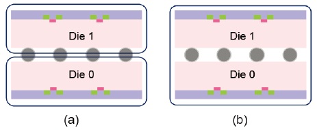
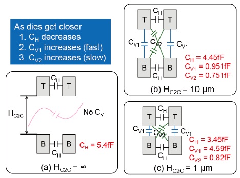
For dense I/Os in F2F-bonded systems, smaller bumps at a lower chip-to-chip height (=HC2C) are inevitable. If the bump size scales but HC2C does not, the aspect ratio (height) of the bumps increases, causing yield problems. However, closer HC2C introduces inter-die capacitance, which is significant in advanced interconnect technologies. Fig. 1 illustrates our motivation. The two boxes on the bottom (B) and the top (T) represent the top metal of the bottom tier and that of the top tier, respectively. All metal layers have a width/spacing/thickness of 1.8 μm/1.8 μm/2.8 μm that represents an industrial interconnect of the top metal. We use Synopsys Raphael for our simulations.
In Fig. 1(a), capacitance is generated only between the same tier (CH, intra-die capacitance) because the distance between the two dies is significantly large. In Fig. 1(b), when HC2C = 10 μm, inter-die capacitances CV1 and CV2 are generated between tiers. Here, CV1 and CV2 are relatively small compared to CH . However, in Fig. 1(c), when HC2C becomes very low (HC2C = 1 μm), CV1 is larger than CH (4.59 fF > 3.45 fF), implying that the inter-tier capacitance becomes significant as HC2C scales. In addition, notice that CH decreases from 5.4 fF to 3.45 fF. This can be attributed to the E-field sharing between the top tier and the bottom tier. When new aggressors (e.g., top-to-bottom) come close to the original aggressors (e.g., bottom-to-bottom) as shown in Fig. 1(b) and (c), the E-field distributes from the original aggressors to the new aggressors because of the change in the distance. Thus, CH decreases and CV increases. Thus, we conclude that 1) CV increases as HC2C scales. In particular, CV becomes significant when HC2C scales to the most advanced F2F bonding technologies (e.g., HC2C = 1 μm). 2) CH decreases with a decrease in HC2C.
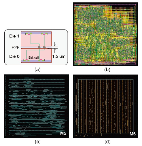
Conventional (=die-by-die) parasitic extraction extracts the intra-die parasitic elements from each die and then stitches them together as shown in Fig. 2(a) [1]. However, if die-by-die extraction is done in 3D designs where HC2C is small, CH is significantly overestimated. Comparing Fig. 1(a) and (c), we find that CH is overestimated by 56.5%. In addition, die-by-die extraction cannot extract CV, which can become larger than CH. Thus, F2F parasitic elements should be extracted in a holistic manner, as shown in Fig. 2(b).
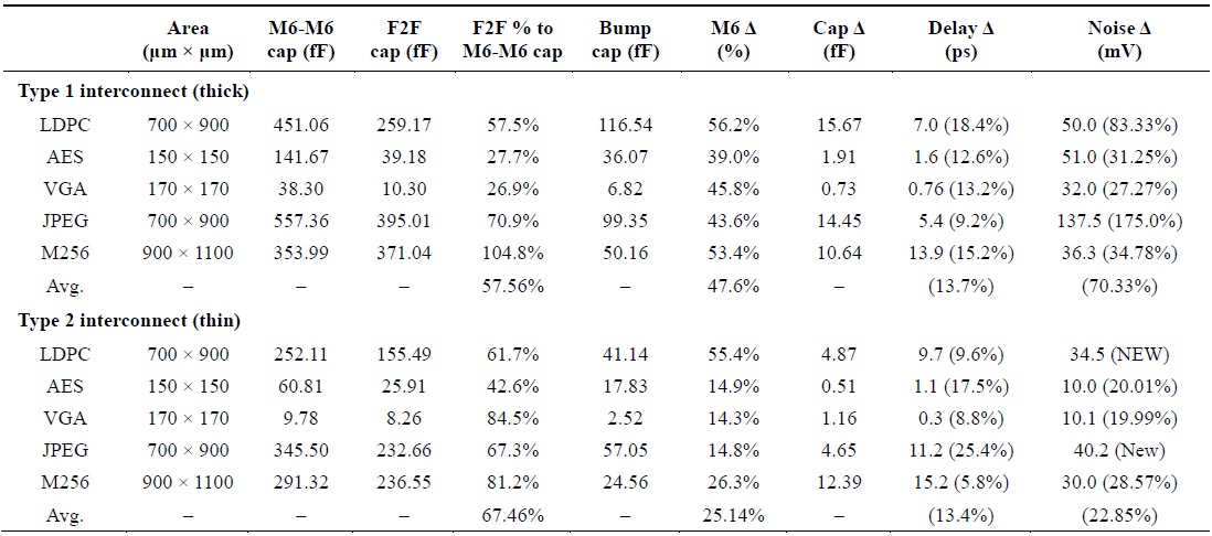
We use Synopsys 28 nm as our baseline process design kit (PDK) [6]. Table 1 describes the two different interconnect structures that we use. We will refer to these structures as Type 1 (thick) and Type 2 (regular), respecttively. Both Type 1 and Type 2 structures consist of six metal layers. The Type 1 structure uses an M6 width/ thickness of 1.8 μm/2.8 μm, and the Type 2 structure uses an M6 width/thickness of 0.36 μm/0.85 μm. For M5, each width/thickness is smaller than M6 and is scaled accordingly on the basis of the M6 width/thickness used. Note that the top metal in both these types of structures represents the dimensions of the actual industrial 28-nm interconnects. For M4 to M1, we follow the interconnects of the Synopsys 28-nm PDK and use the same for both Type 1 and Type 2 structures. For the 3D stack-up, our F2F bump diameter is 1.6 μm [2] and the chip-to-chip distance is 1.5 μm [3]. We assume that when an F2F design is completed in Type 1 (or Type 2), both dies will have the same Type 1 (or Type 2) interconnect structure.
[Table 1.] Interconnect dimensions used in our design
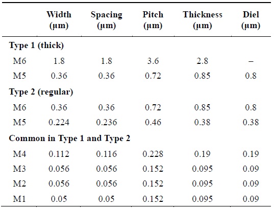
Interconnect dimensions used in our design
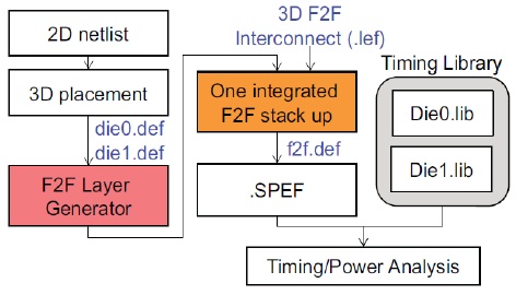
Fig. 3 shows the proposed extraction and analysis flow. First, we partition a two-dimensional (2D) netlist into two tiers and perform placement on each die. Our placer is based on a force-directed 3D gate-level placement engine [7], and it is modified accordingly to perform placement in our F2F design flow. This gives us the placement results for the two tiers (Die9.def and Die1.def). Once the placement is done, we use our F2F layer generator for generating a two-tier holistic F2F stack for routing and extraction. First, our F2F layer generator assigns the standard cells on the top (Die 1) and the bottom (Die 0) of the stack by using the placement from the previous step (Die9.def and Die1.def). Second, the F2F layer generator creates a platform that models all metal layers of both dies and the F2F interface in a holistic manner for the interconnects. Based on our platform, a holistic fullchip F2F-bonded 3D design (f2f.def) can be created in Cadence SoC Encounter (a commercial P&R tool) for fullchip F2F design and impact study.
Given our 3D F2F platform, we use Synopsys StarRC and extract both intra-tier and inter-tier (F2F) parasitic elements in just one run (.SPEF). Further, the fact that our platform is developed using 2D CAD tools does not deteriorate the accuracy of the F2F extraction results because StarRC is a 3D-based EM solver. As long as we feed the correct details of the full-chip F2F design that we have into the solver, the results of our holistic extraction are accurate in the commercial grade. In addition, commercial tools have been proven to be accurate for the extraction F2F parasitic elements [8]. Fig. 4(a) shows the results of our F2F layer generator, and Fig. 4(b) shows a layout shot of the final result (benchmark: AES) after the completion of the 3D design. Once the parasitic elements are extracted, we provide the timing/power library of the standard cells in each die (Die9.lib and Die1.lib) and perform a timing/power analysis by using Synopsys PrimeTime. To focus on visualizing the impact of F2F capacitance on circuits, we do not include any I/Os in our designs.
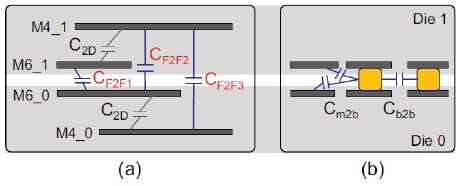
Next, we will introduce the new capacitances formed in F2F 3D ICs. We define these inter-tier capacitances as ‘F2F (3D) capacitances,’ and intra-tier capacitances as ‘2D capacitances.’ Fig. 5(a) shows these F2F capacitances when there are no bumps between the top metals of the chip. Note that F2F capacitances are generated not only between the top metal layers (CF2F1) but also between other metal layers (CF2F2 and CF2F3). In addition, F2F capacitance not only consists of the inter-metal capacitance but also the capacitance from the bumps to the other structures—bump capacitance, Fig. 5(b). Bump capacitance is of the following two types: bump-to-bump capacitance (Cb2b) and metal-tobump capacitance (Cm2b).
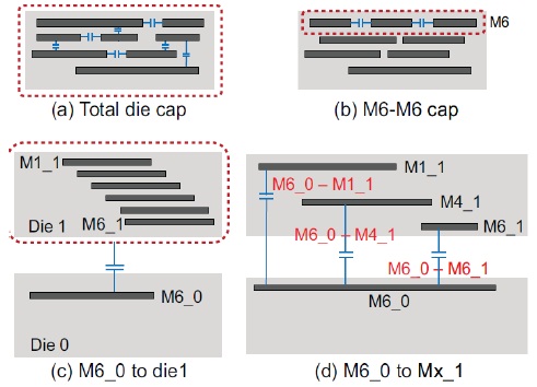
We report how significant F2F capacitance is to the other capacitances in the LDPC benchmark. To explain this, we report three capacitances for comparison: total coupling capacitance inside a die (=total die cap) as shown in Fig. 6(a), M6-to-M6 coupling capacitance generated inside the same die (=M6-M6 cap) as shown in Fig. 6(b), and total F2F capacitance generated between the two dies (F2F cap). Table 2 shows our results. We will now explain the results for the Type 1 structure and then for the Type 2 structure. The total F2F capacitance is 259.17 fF. Note that this is a significant value and cannot be extracted by die-by-die extraction.
[Table 2.] Comparison of face-to-face (F2F) capacitance to the other capacitances
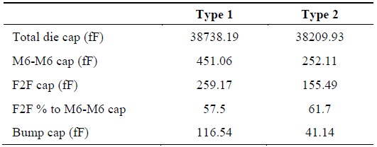
Comparison of face-to-face (F2F) capacitance to the other capacitances
We note the following points. 1) The total coupling capacitance formed in a die is 38738 fF, and compared with this, the F2F capacitance is only 0.67% of the capacitance formed in a single die. 2) However, M6-M6 capacitance in the same die is 451.06 fF. Compared with this, the F2F capacitance is 57.5% of the M6-M6 capacitance. 3) Bump capacitance (116.54 fF = Cb2b + Cm2b) comprises a significant portion of the F2F capacitance. We see a similar trend in the Type 2 structure. The F2F capacitance is 0.41% of the capacitance generated in a single die, but it is 61.7% of the M6-M6 capacitance. The bump cap is also noticeable, which is 26.4% of the F2F cap. The ratio of the bump cap to the total F2F cap in the Type 1 structure is larger than that of the Type 2 structure. Since the metal dimensions of the Type 1 structure are significantly larger than those of the Type 2 structure (Type 1 M6 is 3.3× thicker and 5× wider than Type 2 M6), Cm2b in the Type 1 structure is greater than that in the Type 2 structure. In brief, the F2F capacitance contributes significantly to the total capacitance, and this impact should not be ignored.
We now break down the two types of F2F capacitance. First, we measure the capacitance from one metal (on Die 0) to the other die (Die 1). For example, ‘M6_0–Die 1’ denotes the total capacitance formed between M6 (in Die 0) and all other metal layers in Die 1 (see Fig. 6(c)). Table 3 shows that most of the F2F capacitance is generated between the top metal (M6) and the other die in both types of structures (98.64% in the Type 1 structure and 97.17% in the Type 2 structure). Second, we measure the F2F capacitance between the metal layers. We see that most of the capacitance is generated between the top metal layers of each die (M6_0–M6_1: more than 90%, see Fig. 6(d) for definitions) in both types of structures. This makes sense because M6 is the thickest among all the metal layers, and M6 shields the inter-tier E-field that tries to generate capacitance between the other metal layers. In short, most of the F2F capacitance is generated between the top metal layers.
[Table 3.] F2F capacitance breakdown (see Fig. 6(c) for definitions)
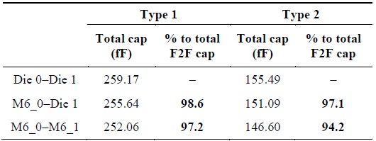
F2F capacitance breakdown (see Fig. 6(c) for definitions)
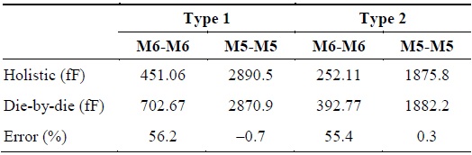
We verify our motivation discussed in Section II on the full-chip scale. We measure the M6-M6 and M5-M5 capacitances (in the same die) and compare the two extraction methods (die-by-die and holistic). Table 4 shows the results. In both Type 1 and Type 2 structures, we report that the die-by-die extraction overestimates the M6-M6 capacitance significantly (56.2% in the case of the Type 1 structure and 55.4% in the case of the Type 2 structure) because of the inter-tier E-field sharing. We report that 1) the M6 capacitance is significantly overestimated in the dieby-die extraction when the inter-tier interaction between metals is not considered in the F2F designs. Note that when the distance between the tiers decreases, the F2F capacitance (CV) increases (see Fig. 1) and, at the same time, the capacitance between metals in the same tier (CH) decreases. 2) The capacitance is significantly overestimated in M6 but not in M5. In short, F2F bonding causes a significant capacitance reduction in the top metal but has an almost negligible impact on the metal below.
Capacitance overestimation in die-by-die extraction because of the face-to-face (F2F) cap in the LDPC benchmark
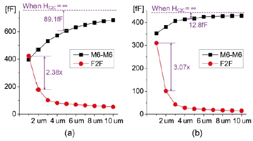
Fig. 7 shows how the capacitances change when the chipto-chip distance (HC2C) changes from 1 μm to 10 μm in both Type 1 and Type 2 structures. It also reports the change in the M6-M6 capacitance in the same die. In both interconnect types, the F2F capacitance converges to 0 and the M6-M6 capacitance saturates to the die-by-die-extracted value as the distance increases (HC2C = ∞). First, in the Type 1 structure, the M6-M6 capacitance reduction shows a steeper slope and starts changing more even at a large F2F distance than in the Type 2 structure. For example, when HC2C = 5 μm, the Type 1 structure shows a –89.1-fF reduction, while the Type 2 structure shows only a –12.8-fF reduction.
Comparing the two interconnect types, we find that the Type 1 M6 has a wider pitch (3.6 μm) than the Type 2 M6 (0.72 μm). Because of this, M6-M6 is relatively loosely coupled (as compared to that in the Type 2 structure) in terms of the E-field strength. Therefore, F2F coupling starts affecting capacitance even from a far distance. Further, the Type 1 structure has an F2F distance to metal pitch ratio of 1.38× (5/3.6) and the Type 2 structure has a ratio of 6.94×. This indicates that the relative F2F distance of the Type 1 structure is 5× closer than that of the Type 2 structure. This is why the M6-M6 capacitance drops faster in the Type 1 structure.
Second, the F2F capacitance increase at a shorter distance (1–2 μm) is higher in the Type 2 structure (3.08×). Type 2 designs are always packed with more M6 objects than the Type 1 designs because of the closer metal pitch in the same area. Therefore, when the chip-to-chip distance is shorter than a certain value where its capacitance increase ratio is significantly high (e.g., 2 μm to 1 μm), the Type 2 structure shows a higher F2F capacitance because it has more M6 objects than the Type 1 structure to generate the capacitance. In fact, note that when HC2C = 1 μm, the F2F capacitance is significant in both types of structures. This implies that the F2F-bonded 3D ICs will suffer more from the F2F capacitance at shorter chip-to-chip distances.
IV. FULL-CHIP TIMING/NOISE IMPACT
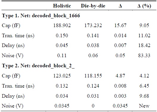
Using the flow from Section III, we use Synopsys PrimeTime for the timing and noise analysis. We perform a static timing analysis (STA) on the basis of the clock frequency of the benchmarks. We analyze the timing and noise results of both the die-by-die extraction and the proposed holistic extraction, and compare each net. Then, we report the worst case nets that show the most discrepancy in terms of the capacitance. Table 5 reports the delay and noise of a net in LDPC when M6 wires are used for its routing. First, for both interconnect types, the die-bydie extraction underestimates the capacitance of a net significantly. In the Type 1 structure, the F2F capacitance is underestimated by 15.67 fF, and this is a 9.05% difference from the value estimated by using the proposed holistic extraction. Because of this, the die-by-die extraction underestimates the transition time and delay by 11.02% and 18.42%, respectively. Similarly, in the Type 2 structure, the capacitance is underestimated by 4.87 fF, and, because of this, both the transition time and the delay are significantly underestimated. Consider that a net on the critical path or a clock net uses the top metal in the F2F design. These nets will have a significant timing error because of the underestimation in the die-by-die extraction, which designers cannot tolerate. Second, die-by-die extraction leads to an inaccurate noise analysis. In the Type 1 structure, the noise voltage of a net is underestimated by 50 mV, and this is 83.3% of the noise missed in the die-by-die method. In the Type 2 structure, die-by-die extraction does not find any effective aggressors near the victim net. However, holistic extraction finds the inter-tier aggressors that die-bydie extraction misses and provides accurate results. Misalignment and process variation between dies (in both the X–Y and the Z direction) causes a significant 3D capacitance change. Stemming from this change, these variations will cause an additional timing/noise error on each net.
[Table 5.] Full-chip timing and noise analysis in the LDPC benchmark

Full-chip timing and noise analysis in the LDPC benchmark
The total power consumption by the two different extraction methods is almost the same. For example, Type 1 LDPC consumes 49.5 mW in die-by-die extraction and 49.7 mW in holistic extraction. Type 2 LDPC consumes 49.0 mW in die-by-die extraction and 49.1 mW in holistic extraction. This is a less than 1% difference. This difference can be attributed to the following. (1) Despite the increase in the F2F capacitance due to F2F bonding, the intra-die capacitance (CH in Fi. 1) decreases at the same time. (2) In terms of the total capacitance in the full-chip, the portion that the F2F capacitance contributes is very small. In addition, since the M6-M6 capacitance decreases at the same time, the total capacitance difference between die-bydie extraction and holistic extraction at the full-chip level is almost negligible (less than 0.1% in total). The dynamic power in digital circuits can be expressed by the following equation:
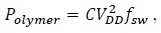
where C denotes the capacitance, VDD represents the supply voltage, and fsw indicates the operating frequency. Since the change in the total capacitance is less than 0.1% in total, which is the only changing parameter between the two extraction methods, the power difference from die-by-die extraction and holistic extraction is almost negligible.
We use five benchmarks (including LDPC) to estimate the impact of F2F parasitic elements in various full-chip designs [5]. The biggest benchmark JPEG consists of 226 K cells, which is more than 1 M transistors, and the smallest benchmark VGA consists of 5.5 K cells. Benchmarks are sized optimally to perform routing without any violations. Table 6 reports our comprehensive results. Through many benchmarks, we report that 1) the portion of F2F capacitance in the M6-M6 capacitance is significant (>67% on average in Type 2 structures), and the bump cap is a big contributor to the total F2F cap. 2) Die-by-die extraction significantly overestimates the M6-M6 capacitance (M6 error, >47% on average in Type 1 structures) but not much on other layers. 3) PDN reduces the F2F capacitance significantly (>47% on average in Type 2 structures). 4) The capacitance error on nets occurs in full-chip designs when using die-by-die extraction. Because of this, the underestimated total capacitance causes significant timing (25.48%) and noise (175%) errors on the nets.
[Table 6.] Results for all benchmarks
Results for all benchmarks
In this paper, we proposed a holistic parasitic extraction methodology for F2F-style 3D ICs. We found that these inter-tier parasitic elements become non-negligible, and these parasitics significantly change the capacitance values of the top metal on each die. We demonstrated that a shorter F2F distance causes a significant error in the M6-M6 capacitance (56.2% in LDPC) and a considerable increase in various inter-tier capacitances that the die-to-die extraction cannot extract (104.8% of M6-M6 in M256). Among all these F2F capacitances, we found that the M6_0-M6_1 capacitance is the most significant contributor to the total F2F capacitance. We also found that die-by-die extraction 1) significantly overestimates the M6-M6 capacitance (in the same die) and 2) cannot accurately extract the F2F capacitance. Because of this, a significant timing/noise error occurs (25.48/175%) in the nets. With respect to the reduction in the F2F capacitance, we found that PDN can reduce it significantly (–58.3% in M256).