Recently, because of the advancement of electronic and communication technology, the control of electromagnetic (EM) wave environments has become an important issue. Thus, countermeasures against electromagnetic interference (EMI) and electromagnetic susceptibility (EMS) are urgently required [1]. The recommendations and regulations for EM wave environments have been established and enforced from 1970 by the Comité International Spécial des Perturbations Radioélectriques (CISPR), the Federal Communication Commission (FCC), the Voluntary Control Council for Interference (VCCI), the German Verband Deutscher Elektrotechniker (VDE), and the Conformite Europeenne (CE) mark [2, 3].
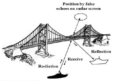
Nowadays, many extensive studies on countermeasures against electromagnetic compatibility (EMC) problems have been carried out. As an example of EMC problems, which consist of those related to noise, victim, and propagation path, Fig. 1 shows the occurrence of a false echo on a ship’s radar. This can be eliminated by attaching an EM wave absorber on the bridge surface. To solve EMC problems, one of the EMC components has to be controlled. For the control of three components of EMC, variable countermeasure techniques are used, such as filtering, cabling, grounding, isolating, and shielding [4, 5]. Although some shielding methods can control noise problems, they cause other problems due to reflection waves. Thus, EM wave absorbers have recently been attracting public attention since they can essentially control the noise, victim, or propagation path from unnecessary waves.
In this paper, first, we introduce some countermeasure methods against EMI/EMC. Then, the smart EM wave absorber was designed, which has heat radiating function, absorption ability of more than 20 dB in the frequency band of 2–2.45 GHz, optimum aperture (hole) size, space between adjacent holes, and hole thicknesses of 6 mm, 9 mm, and 6.5 mm, respectively.
II. RESEARCH WORKS ON EM WAVES AT KMOU
Although countermeasure techniques for EMC problems adopt various methods such as filtering, cabling, absorbing, grounding, isolating, and shielding, recently, the EM wave absorber has attracted maximum public attention because it can essentially eliminate the unnecessary EM waves. The following paragraphs introduce several types of EM wave absorbers that are being developed by our research team.
Recently, EMI problems have been found to occur because of the miniaturization of the IC technology by the use of high frequencies. These problems are caused by the coupling between adjacent devices or cables. Moreover, the current from a high-speed clock and pulsed data signals in printed circuit board (PCB) produce strong conducted emission and radiated emission in a broad frequency band. Although filtering and absorbing are used to solve these problems, this work is focused on EM wave absorbers. An EM wave absorber is applied by attaching on an IC package, a flat cable, signal line, and the cover of PCB to eliminate noise [6]. In our laboratory at the Korea Maritime and Ocean University (KMOU), we have developed a sheet-type EM wave absorber for PCB. The most recently developed EM wave absorber has a thickness of 0.85 mm and an absorption ability of 5.4 dB at 2.4 GHz, and exhibits an adsorption ability of more than 3 dB in the frequency band of 1.4–4.1 GHz. Sendust and Mn–Zn ferrite were used as the magnetic loss materials, and chlorinated polyethylene (CPE) was used as the binder. The EM wave absorber was made of sendust, Mn–Zn ferrite, and CPE (sendust:Mn–Zn ferrite:CPE = 70:5:25 wt%).
>
B. EM Wave Absorber for Electric Toll Collection System
A metropolis is faced with serious traffic congestion problems as a result of societal and economic growth. Thus, the government has introduced an intelligent transport system (ITS) as a solution to these problems. As an example of ITS, an electronic toll collection (ETC) system may realize it. The ETC system is a non-stop auto-collection system and is an application of dedicated short-range communication (DSRC) using a microwave frequency of 5.8 GHz. ETC is a communication system between a roadside antenna at the toll gate and a vehicular antenna inside the car. When the ETC system is working, communication errors are caused in the ETC environment due to undesired EM waves reflected by walls, ETC gates, or the other possible nearby objects (e.g., a canopy or a road surface). These problems can be solved using an EM wave absorber. In other words, an optimal use of the EM wave absorber can mitigate these problems. Therefore, several types of EM wave absorbers are used in various places [7].
>
C. EM Wave Absorber for Wireless LAN
Recently, a wireless LAN has often been applied at a home or in an office because of its several convenience merits, the frequency band of which is from 2.4 GHz to 5.2 GHz, and is specified in IEEE 802.11a and IEEE 802.11b [1]. When a wireless LAN system is in operation, problems such as deterioration of transmission speed by multipath fading and communication errors occur. The multipath problem is caused by undesired EM waves reflected from walls, ceiling, and ground; these undesired EM waves attenuate the original signal. An EM wave absorber has been proposed to solve this problem. Since the EM wave absorber can eliminate the undesired EM waves, a better communication environment is offered.
Sheet-type EM wave absorbers have been developed for wireless LAN. The most recently developed EM wave absorbers have a thickness of 3.7 mm and an absorption ability of 17 dB at 2.4 GHz, and a thickness of 3.8 mm and an absorption ability of 23 dB at 5.2 GHz. The EM wave absorber for wireless LAN at 2.4 GHz is made of Mn–Zn ferrite, carbon, and CPE (sendust:Mn–Zn ferrite:CPE = 16:64:20 wt%). For the frequency of 5.2 GHz, the EM wave absorber is made of Mn–Zn ferrite, carbon, and CPE (Mn– Zn ferrite : carbon : CPE = 40:15:45 wt%). Sendust and Mn–Zn ferrite are used as magnetic and carbon is as conductive loss materials, and CPE is used as the binder.
A sheet-type EM wave absorber for the ceiling of ETC has been developed. The most recently developed EM wave absorber for the ETC ceiling has a thickness of 3.38 mm and an absorption ability of 23 dB at 5.8 GHz. The EM wave absorber for the ceiling of ETC is made of Mn–Zn ferrite, carbon, and CPE (sendust:Mn–Zn ferrite:CPE = 40:15:45 wt%). Mn–Zn ferrite is used as the magnetic loss material, carbon as the conductive loss material, and CPE as the binder.
>
D. EM Wave Absorber for RFID System
The dense mode of radio-frequency identification (RFID) systems in a warehouse or harbor, where hundreds of antennas are positioned in a small area, causes the interferences between all readers and tags. Thus, to avoid a severe communication interruption, the interferences between RFID systems must be removed carefully.
We have developed a sheet-type EM wave absorber for RFID tags. The most recently developed EM wave absorber has a thickness of 4 mm and an absorption ability of 25 dB at 940 MHz. The EM wave absorber for RFID tags is made of an amorphous metal and CPE (amorphous:CPE = 80:20 wt%). The amorphous metal is used as the magnetic loss material, and CPE is used as the binder.
III. EM WAVE ABSORBER WITH HEAT DISSIPATING FUNCTION
>
A. CNT or CNF as an Absorption Material
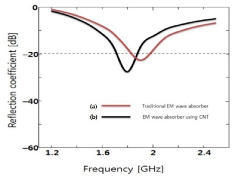
Carbon, permalloy, ferrite, sendust, soft magnetic metals, etc., are often used as conventional EM wave absorbing materials that have imaginary parts in their material constants. These materials have relatively good absorption properties but have a limited absorbing frequency band and absorption ability [4]. In this research, thus, carbon nanotubes (CNTs) were used as an absorbing material to overcome the bandwidth limitation. Fig. 2(a) shows the absorption characteristics for the conventional EM wave carbon absorber and Fig. 2(b) shows those for the CNT absorber. From Fig. 2, we can see quantitatively that the CNT absorber exhibited better improvement than the conventional EM wave carbon absorber from the perspective of absorption bandwidth and absorption ability.
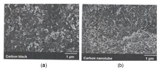
Fig. 3 shows the scanning electron microscope (SEM) photographs of carbon black and CNT materials. The carbon black considered in Fig. 3(a) is a fine carbon powder equivalent to the so-called carbon soot particle size of 0.3 mm. Fig. 3(b) shows the SEM photograph of CNTs made of combinations of carbon or the other carbon atoms.
The considered CNT has a diameter of 0.01 μm and occupies only a small area of the composition. In general, CNTs have excellent mechanical properties and field emission characteristics of electrical-selective, exceptionally high-efficiency hydrogen storage characteristics, and defects of the existing substance, which are known to be a perfect little new material [5, 6]. Currently, carbon nanofibers (CNFs) are used in secondary batteries, semi-conductor materials, etc.
An important challenge for the future is to adopt nanotechnology (NT) and electromagnetic wave technology (EMW technology) to develop NT-based high-performance composite fusion technology, and to develop an EMW smart absorbing body.
Further, CNTs have mirror symmetry, which can be used to control their electrical properties. Since In particular, the geometric symmetry with this atom-like Missy in the system affects on the kind of CNT material [7], it is very important choose appropriate shapes, sizes, etc [8, 9]. Further, smart EM wave absorbers with CNFs have been studied in this research.
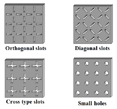
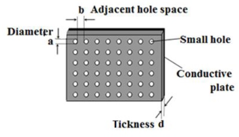
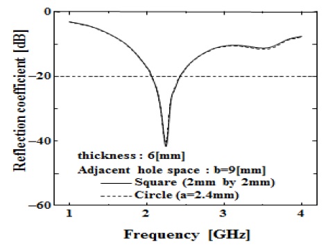
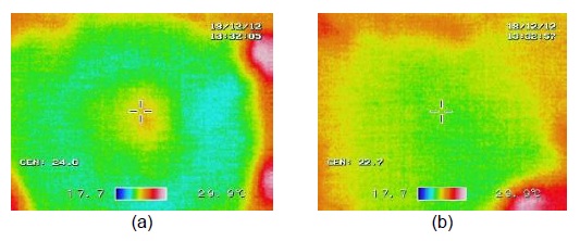
Fig. 4 shows wave absorbers of various shapes. Firstly, in this paper, the form of a circular hole [10] was proposed and considered by simulating the absorption performances. As shown in Fig. 5, the dimensions of d, a, and b depict the thickness of the absorber, the diameter of the hole, and the interval between adjacent holes, respectively. Fig. 6 shows the heat radiating degree for the absorbers with the apertures forming as in Fig. 6(a) and without the apertures as in Fig. 6(b), respectively. From the above, it was clearly shown that heat radiation ratio in the case with the apertures is higher than in the case without the apertures. Fig. 7 shows the changes in the absorption characteristics according to the change in the hole space when the thickness and the size of the holes were fixed.
>
B. Performance Improvement by Virtue of the Apertures
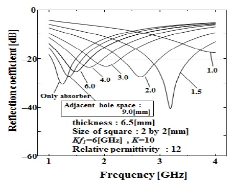
We performed some simulations for the evaluation of the above facts. Based on the simulation results, the absorption characteristics of the absorber suitable for the band of 2 GHz to 2.45 GHz were calculated; all the absorbers and the holes are depicted in Fig. 8. The finally designed absorber can absorb more than 20 dB and has excellent absorption characteristics.
Recently, technical progress has led to the development of sophisticated electronic products and systems. Therefore, demands on designers to ensure EMC have increased. Although there are several methods to protect products or humans from unwanted EM waves, EM wave absorbers are coming into the spotlight.
Various types of EM wave absorbers have now been developed or are in progress. In this paper, we introduced some EM wave absorbers that are being developed, such as EM wave absorbers for PCB, ETC, wireless LAN, and RFID systems. These EM wave absorbers have been fabricated as sheet-type devices.
We confirmed that the heat radiating degree for the absorbers varies with dependence on whether apertures were formed or not. It was shown that the heat radiation ratio was improved by forming the apertures and higher than in the case of no apertures. The absorption characteristics were changed according to the hole space in spite that the thickness and the size of the holes were fixed.
Furthermore, some simulations were carried out to confirm the above facts. Based on the simulation results, the absorber dimensions suitable for the frequency band of 2 to 2.45 GHz were derived and the characteristics of the designed absorber were calculated. The finally designed one could absorb more than 20 dB and has the excellent absorption characteristics.