This paper reports the optimized mixed-signal performance of a high-voltage (HV) laterally double-diffused metaloxide-semiconductor (LDMOS) field-effect transistor (FET) with a dual gate oxide (DGOX). The fabricated device is based on the split-gate FET concept. In addition, the gate oxide on the source-side channel is thicker than that on the drain-side channel. The experiment results showed that the electrical characteristics are strongly dependent on the source-side channel length with a thick gate oxide. The digital and analog performances according to the source-side channel length of the DGOX LDMOS device were examined for circuit applications. The HV DGOX device with various source-side channel lengths showed reduced by maximum 37% on-resistance (RON) and 50% drain conductance (gds). Therefore, the optimized mixed-signal performance of the HV DGOX device can be obtained when the source-side channel length with a thick gate oxide is shorter than half of the channel length.
The design of integrated circuits (ICs) has shifted toward the multi-functional and mixed-signal system-on-a-chip (SoC), which has many benefits, such as a smaller system size, competitive cost, secured system information, and lower power consumption. Generally, electronic systems require multi-voltage signal processing due to the various peripherals in the real world. Therefore, for the mixed-signal SoC design, high-voltage (HV) devices are required for input/output interface circuits with offchip components, such as sensors, power switches, actuators, and motors [1-3]. The integration of HV devices with advanced low-voltage (LV) complementary metal-oxide semiconductor (CMOS) devices can achieve full system integration. For the integration of HV devices, laterally double-diffused MOS (LDMOS) transistors are favorable because of their good compatibility with modern standard CMOS processes [4].
Recently, several groups have proposed a range of LDMOS structures to improve their device performance [5-14]. In advanced reduced surface field (RESURF) technologies and fieldplate gate structures, attention has been paid to the reduced device size and on-resistance (RON) while maintaining the breakdown voltage (BV) [5]. These techniques are effective only for the switching characteristics of power ICs. Alternatively, some LDMOS devices using gate and channel engineering have been reported [6-12]. These LDMOS devices are based on the split-gate field-effect transistor (SGFET) concept [13]. The main idea of the SGFET concept is modulation of the channel inversion charge density. Therefore, the SGFET has a resistive channel on the source side and conducting channel on the drain side. The modulated channel potential due to the asymmetric channel resistance can improve the device performance. One of the implementations of LDMOS devices through gate engineering showed improved device performance for mixed-signal applications [6-9]. Another LDMOS device with a lateral asymmetric channel (LAC) was also shown to improve the electrical characteristics [10-12]. Based on the SGFET concept, the channel inversion charge density can also be modulated by the gate oxide thickness. The LDMOS device with a dual gate oxide (DGOX) using a HV CMOS process exhibited better transconductance (gm) and drain current driving characteristics [14]. On the other hand, they focused only on the DGOX LDMOS device concept and the experimental electrical characteristics for circuit applications are still insufficient.
Focusing on mixed-signal circuit applications, this paper presents in more detail the electrical characteristics of HV LDMOS transistors with a DGOX structure and its performances are compared to conventional devices with a single gate oxide (SGOX). The DGOX LDMOS devices were fabricated using a 0.18-μm 20-V HV CMOS process without special processing steps. A two-dimensional (2D) device simulation was also performed to optimize the electrical characteristics of the fabricated devices.
2. DEVICE STRUCTURE AND FABRICATION
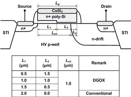
Figure 1 presents a cross-section of the fabricated LDMOS transistors and design information. The DGOX LDMOS devices had a thick gate oxide of 50 nm thickness at the source side (L1) and a thin gate oxide of 7 nm thickness at the drain side (L2). The polycrystalline silicon (poly-Si) gate length (Lg = L1 + L2) and overlap length (LO) of the gate and the n-drift region of the fabricated devices were 2.0 and 0.2 μm, respectively. The channel width (W) and length (Lch) were 20.0 and 1.8 μm, respectively. The sourceside channel length with a thick gate oxide (L1) was varied from 0.5 to 1.5 μm to obtain the optimal performance for mixed-signal circuit applications and to provide a guide for process control for lithography misalignment and isotropic wet etching variations. The conventional LDMOS device with a single gate oxide (L1 = 2.0 μm) was also fabricated for a comparative study. The fabricated conventional device had identical dimensions and junction profiles, except for the gate oxide structure.
The dual gate oxide process is commonly used for modern CMOS technologies because of the high power supply and interface with high-voltage operation of off-chip components. A 0.18-μm CMOS technology with an embedded 20-V class HV device was applied for fabrication. Therefore, no additional process step was required for the device fabrication.
The major process flow was as follows. First an HV p-well was formed on a p-type substrate. A conventional shallow trench isolation process was performed for device isolation. A lightly doped n-drift layer was formed on the HV p-well region. A retrograded p-well region was also formed for a low-voltage device. Buffer oxidation (46 nm), photolithography, and wet etching using a buffered-oxide-etch solution were performed sequentially. The final thicknesses of the thin and thick gate oxides are 7 and 50 nm, respectively. Undoped poly-Si (250 nm) was deposited and patterned using dry etching. After gate patterning, a lightly doped drain (LDD) junction was formed. SiO2/Si3N4 (15 nm / 55 nm) dielectrics are applied for the LDD spacer, and source and drain junction ion implantation was then performed. A cobalt silicide (CoSi2) layer was formed for the active and gate regions. TEOS oxide and chemical mechanical polishing processes were performed for the poly-to-metal layer. The contact formation and single level metal (Al-1%Si) interconnection process were then carried out.
3.1 Two-dimensional (2D) device simulation
A 2D device simulation was performed using MEDICI to clarify the electrical characteristics of the fabricated LDMOS devices [15]. The device simulation structures were the same as that shown in Fig. 1. Briefly, the channel region ranged from 1.0 to 3.0 μm. The surface doping concentration of the HV p-well was 2×1016 cm−3. The electrical gate oxide thickness at the source and drain side was 50 and 7 nm, respectively
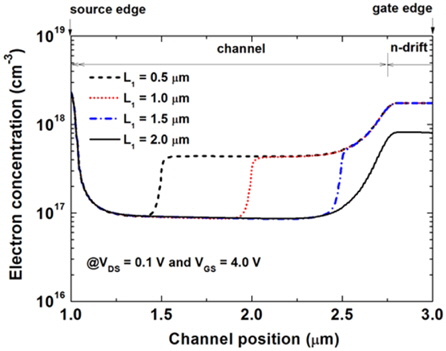
Figure 2 shows the channel electron concentration along the channel of the LDMOS devices at 10 nm beneath the Si/SiO2 interface. The applied bias conditions were VDS = 0.1 V and VGS = 4 V. The gate oxide thickness is a major factor of the threshold voltage (VT). The thin gate oxide region (L2) had a negative VT, and a channel inversion layer had previously formed at a low VGS. As a result, the DGOX devices with L1 = 0.5, 1.0, and 1.5 μm have a step inversion charge distribution along the channel direction. The drain-side channel resistance (Rch.D) of the DGOX devices was much lower than the source-side channel resistance (Rch.S) because of the higher channel electron concentration of the channel under the thin gate oxide region. The total channel resistance is the sum of the source and drain-side channel resistance (Rch.total = Rch.S + Rch.D). Therefore, a shorter L1 length can decrease the total channel resistance of the DGOX device.
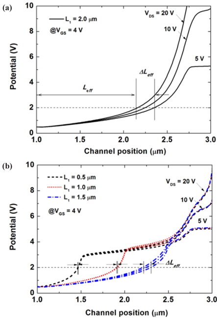
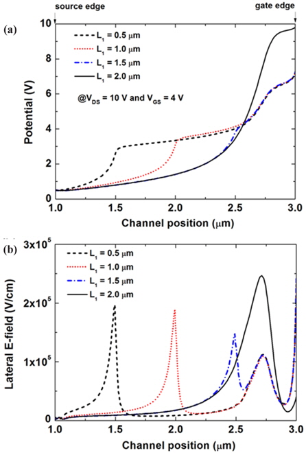
Figure 3 shows the 2D device simulation results of the saturation regime. The bias conditions were VDS = 10 V and VGS = 4 V. The modulated channel resistance of the DGOX devices resulted in a step potential distribution along the channel, as shown in Fig. 3(a). The conventional LDMOS device (L1 = 2.0 μm) showed a typical channel potential distribution; it increases monotonously along the channel region and changed rapidly near the n-drift junction. The step potential distributions of the DGOX devices resulted in a locally enhanced lateral electric field in the channel. Fig. 3(b) also shows additional electric field peaks at the L1/L2 borders. The locally enhanced electric field can improve the carrier velocity [14]. Hence, drain current improvement was expected in the DGOX devices, and a short L1 length revealed improved transport characteristics. In addition, the DGOX devices exhibited a reduced lateral electric field at the n-drift edge because the electric field is redistributed by the step potential change of the DGOX structure. Moreover, such reduction in the lateral electric field at the n-drift edge can increase the channel hot-carrier immunity [16].
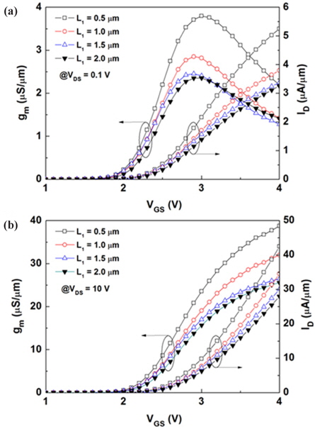
Figure 4 shows the measured gm-VGS and ID-VGS characteristics of the fabricated LDMOS devices. In the triode regime (VDS = 0.1 V), the measured VT values of the fabricated LDMOS devices increased slightly from 2.09 V to 2.17 V with increasing L1. The LDMOS devices with a longer L1 required a higher channel inversion charge to switch on the device. VT was measured at a constant ID = 1.0 μA. In the triode regime, as shown in Fig. 4(a), gm increases gradually and reaches the maximum value. As VGS increases, gm decreases monotonically due to the inversion carrier mobility reduction. The DGOX device with a shorter L1 showed a larger maximum transconductance (gm.max) in the triode regime. The gm characteristics were improved due to the higher drain current (ID). The gm.max of the DGOX device with L1 = 0.5 μm was improved by 61.1% compared to the conventional device. In the saturation regime (VDS = 10 V), the DGOX device also showed improvement in the gm and ID, as shown in Fig 4(b). The ID of the DGOX device with L1 = 0.5 μm was improved by 51.7%, compared to the conventional device. As shown in Fig. 3, the locally enhanced electric field in the channel can assist in the carrier velocity improvement. The carrier velocity was enhanced more with a shorter L1 because of the lower channel resistance, as discussed in Fig. 2. Therefore, the gm and ID improvements in the DGOX devices are strongly dependent on the L1 length.
3.3 Breakdown and on-resistance characteristics
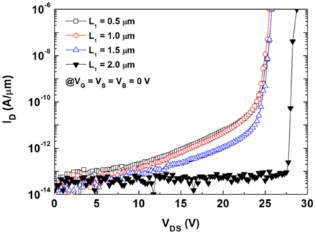
Figure 5 shows the measured breakdown characteristics of the fabricated LDMOS devices at the off-state (VG = VS = VB = 0 V). The measured breakdown voltage (BV) of the conventional device was 28 V. The BV was measured at ID = 10 nA/μm. For the DGOX devices, the drain current increased gradually from VDS = 10 V and the breakdown occurred at approximately 25 V due to an increase in tunneling of the thin gate from VDS = 10 V. The ndrift junction of the applied process was not optimized for the thin gate oxide structure. These BV characteristics of the DGOX devices might be minimized by n-drift doping control for lateral electric field reduction.. In addition, these leakage characteristics can be adjusted by the multiple steps of the gate oxide. A good example was suggested in previous literature [16].
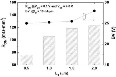
Figure 6 shows the specific on-resistance (RON) characteristics as a function of the L1 length at VDS = 0.1 V. RON is an important parameter in the switching operation of HV devices, and is inversely proportional to the triode ID shown in Fig. 4(a). A lower RON of the DGOX device with a shorter L1 can be expected because of the enhanced ID with a shorter L1. The RON of the HV device is dominated by the channel and n-drift resistance [17]. Therefore, lowering the channel resistance is an effective way to reduce the RON value. The DGOX device with L1 = 0.5 μm showed the lowest RON, which was reduced by 37.7% compared to the conventional device at VGS = 4 V. The trade-off between BV and RON is a major issue for HV devices for switching applications. Considering a BV reduction of 3 V, the DGOX device with a shorter L1 has a comparably lower RON than the conventional device.
3.4 Drain output characteristics
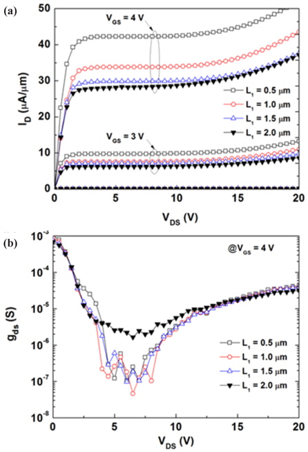
Figure 7 shows the measured ID-VDS and drain conductance (gds) characteristics of the fabricated LDMOS devices. The DGOX devices showed higher drain current capability than the conventional device, as shown in Fig. 7(a). The device simulations and measurements showed good agreement with the ID improvement in the DGOX device. The ID of the DGOX device with L1 = 0.5 μm showed 48.2% improvement compared to that of the conventional device at VDS = 10 V and VGS = 4 V. On the other hand, it is difficult to apply a higher gate voltage (VGS > 4 V) to the DGOX device due to the 7 nm thin gate oxide at the drain-side channel. On the other hand, the conventional device with a 50 nm thick gate oxide supports gate voltages of up to 20 V. Some applications, such as the HV available input interfaces, charge pump, and output drivers for flat panel displays require a high gate voltage. A higher drain current can be achieved at a higher VGS compared to the DGOX device. Therefore, conventional devices are generally used for output drivers in mixed-signal ICs. The disadvantage of conventional devices is the additional circuitry, such as the level shifter.
The DGOX device can be considered to be an analog friendly device and has some advantages for circuit design. The DGOX devices, which are interfaced with the LV devices without a level shifter, operate normally in the saturation regime (VDS > VGS - VT). Considering the analog friendly devices, this study examined the drain conductance (gds) characteristics of the fabricated devices. The drain conductance is an important parameter for many analog circuit applications. As shown in Fig. 7(b), the DGOX devices showed lower gds than the conventional device in the saturation regime. The gds was lower in the saturation regime dominated by channel length modulation (CLM) and drain-induced barrier lowering (DIBL). Therefore, the DGOX devices undergo a suppressed CLM and DIBL. In addition, all the fabricated LDMOS devices showed increased ID and gds characteristics at a high drain voltage (VDS > 10 V) due to the substrate current induced body-effect [18]. High-field charge multiplication results in a substrate current, which increases the substrate potential due to the substrate resistance. This substrate potential will reduce the VT and increase the ID characteristics. Hence, gds is also increased.
The suppressed CLM and DIBL mechanism of the DGOX devices can be explained by the screening effect [19]. Fig. 8 shows the 2D device simulation results of the HV devices with various drain voltages. The applied drain voltage was varied from 5 to 20 V at VGS = 4 V. For the conventional device, the drain potential expands toward the channel region at high VDS, as shown in Fig. 8(a). This potential expansion can decrease the effective channel length (Leff) and increase the effective channel length variation (ΔLeff). Therefore, the conventional device shows high gds characteristics, as shown in Fig. 7(b). On the other hand, for the DGOX devices, the step potential change in the channel prevents the expansion of the depletion width induced by the large drain voltage. Most of the drain potential can be screened at the L1/L2 border, as shown in Fig 8(b). Therefore, the DGOX device has a smaller ΔLeff than the conventional device. The CLM is thus suppressed effectively. All the DGOX devices showed similar gds characteristics to those of the measurements.
3.5 Comparison of the analog performance
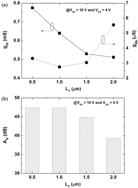
For many analog circuit applications, gm and gds are important parameters. Another key parameter is the intrinsic gain (AV) of the device, which is needed to obtain high performance [20]. Normally the gate bias is much lower than the drain bias for saturation mode operation. Fig 9(a) shows the gm and gds as a function of the L1 length in the saturation regime (VDS = 10 V and VGS = 4 V). As discussed earlier, the DGOX devices showed improved gm and reduced gds characteristics. In addition, the gm was improved further in the DGOX device with a shorter L1 length. The gm of the DGOX device with L1 = 0.5 μm was improved by 52% compared to that of the conventional device. On the other hand, the DGOX device showed similar low gds characteristics. The gds of the DGOX devices was reduced by approximately 50% compared to that of the conventional device. Fig. 9(b) shows the intrinsic gain of the HV devices. The AV (= gm / gds) of the devices was extracted from the measured gm and gds in Fig 9(a). The improved gm and reduced gds characteristics of the DGOX devices can enhance the AV. The AV values of the DGOX devices with L1 = 0.5 and 1.0 μm were identical (47 dB), which is 8 dB higher than that of the conventional device.
This study examined the electrical characteristics of HV MOSFETs to determine the geometric effects of the dual gate oxide structure. The different gate oxide thicknesses affect the threshold voltage and channel potential distribution. The 2D device simulation and measurement results show that the source-side channel length with a thick gate oxide is a strong factor for performance variation. The optimized mixed-signal performance of the HV DGOX device was obtained when the source-side channel length with a thick gate oxide was less than half the channel length. Therefore, the source-side channel length is a device optimizing parameter for mixed-signal circuit applications.
Although the HV DGOX device shows several weaknesses such as low applicable gate voltage and device uniformity due to process variation, we expect that the proposed device structure could be another candidate for high-performance mixed-signal IC design.