Over recent years, microelectromechanical system (MEMS) based devices especially radio frequency (RF) switches have attracted much attention from both academics and industrial experts. RF-MEMS switches replaced the conventional semiconductor based devices like gallium arsenide field-effect transistors (GaAs FETs), metal-semiconductor-field-effect transistors (MES-FETs) and p-i-n diode switches. RF MEMS has many advantages, including high isolation, low insertion loss, excellent linearity and negligible power consumption [1].
Usually, MEMS switches are fabricated using surface micro-machining processes and have a suspended thin metal membrane (fixed-fixed or cantilever), which activates or deactivates the RF signal transmission through mechanical movement of the beam above the signal line of the co-planar waveguides [2,3].
Deposition-based processes have some limitations that can complicate the process of fabrication and, thus, affect performance inherently [4]. Limited layer thickness limits the restoring force and stiffness in MEMS structures. Moreover, there is also a need for switches that can be used for low voltage application. Such requirements limit the use of conventional MEMS designs [5].
Researchers have proposed various designs that solve the MEMS issues [6]. Various types for RF MEMS switches address issues like low voltage and reliability concerns, because the primary engineering concepts only deal with the design of the beam. We have presented the design of a capacitive shunt type RF MEMS switch that not only addresses these concerns but also requires very low operation voltage because it is compact [7,8].
This paper presents a compact and capacitive/shunt RF MEMS switch for Q-band operation [9]. Being a compact switch, this switch shows prominent performance in the higher frequency region. Increasing the electrodes area can compensate for the issue of high actuation voltage but then it also limits the compact switch design. Thus, in this paper the switch membrane is designed with a small footprint. The inclusion of meanders on all sides helps to lower the effective spring constant and stress in the membrane and further provides a good mechanical restoring force. The proposed switch design shows excellent performance in the Q-band frequencies and performance for various other bands is also given in a tabular form. Stress and voltage requirements are computed using a finite element modeller (FEM) [10].
The theory section provides the analytically modeling of various aspects of the switch. However in [5], various aspects have been covered in detail, but the theory is provided as a reference for readers regarding the issues in RF MEMS. These formulas are also used to model switches in the FEM for the computation of various solutions to the problem.
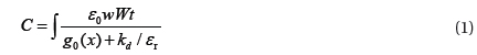
Basically, the electrostatic fields that can be modelled locally in a one-dimensional capacitor model can be analysed. The capacitance is given by the following equation that defines the integral over the overlap area between the membrane and signal line. However, the error introduced by this one-dimensional model is usually less than 5%.

where, ε0 is the permittivity of air, w is the length of the overlapping area and W is the width of the overlapping area, while, t is the thickness of the membrane. g0(x) is the gap between the membrane and the dielectric layer over the signal line, kd is the depth of the dielectric layer and εr is the dielectric constant.
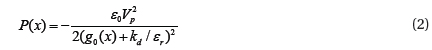
Electrostatic forces on the membrane in the overlap area at the actuation voltage Vp are described by the pressure P, which can be given by and defined as an FEM expression. P is used as a load in the solution of a given problem in FEM.

The integrand of Eq. (1) can also be defined as an FEM expression that can further be numerically integrated to obtain capacitance.
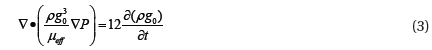
The damping or squeeze film damping that can further dominate the performance of the RF MEMS switch is driven by the vertical motion of the membrane and is caused by the viscosity and inertia of the gas that is squeezed in or out of the in between gap of the membrane and dielectric layer on the signal line. It is described by the Reynolds equations as:

where P is the pressure of gas, g0 is the air gap, μeff is the density of the gap and μeff is the effective viscosity that takes into account the small scale of the air gap that is 3 μm in this case and is approximated analytically by:
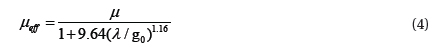
where, λ is the mean free path of the gas in the air gap at ATP. The mean free path λ is approxmately 70 nm. At very slow transients, the time derivative in Eq. (3) is dominated by the variation in the air gap, g0 while the variation in the density of gas plays a crucial role at high frequencies. This is investigated in [5] for the parallel-plate system assuming a variation of a small air gap. The following corner frequencies are derived by:

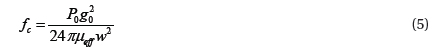
where P0 is the surrounding pressure, w is the width of the overlapping area, and the gas is assumed to be isothermal. Below this frequency, Eq. (3) can be simplified by eliminating the density constant Q.
3. STRUCTURE AND PRINCIPLE OF OPERATION
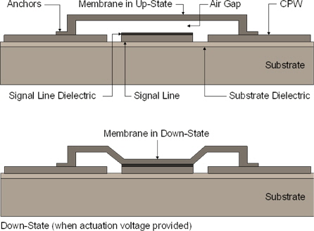
The proposed RF MEMS switch is designed on a 200 μm thick substrate of quartz material which serves as the base of the RF MEMS switch. Co-planar waveguides (CPW) are used for RF signal transmission from the input port to the output port. A high-k dielectric layer of hafnium dioxide (HfO2) is applied over the substrate. The operation principle of the proposed switch is the same as the typical shunt type fixed-fixed beam RF MEMS switch and is shown in Fig. 1. The CPW is characterized at Z0=50:Ω for ease in coupling with coaxial cables.
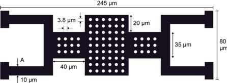
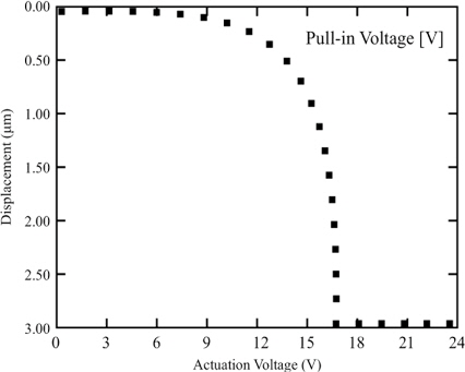
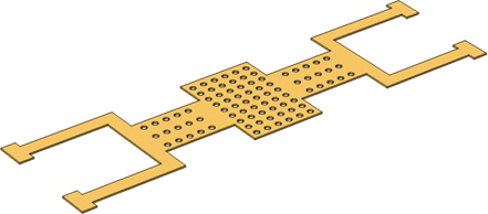
As the membrane has a compact design, the central signal line is optimized with a G/S/G of 40/75/40 . The beam is suspended using crab type meanders connected to four anchors. To lower the pull-down voltage, two 40 μm wide electrodes are used for electrostatic actuation. A gap height of 3 μm is maintained between the central part of the membrane and the RF signal line. The gap height is optimized and selected using pull-in voltage analysis in a finite element modeller. If the gap height was lower than this value, the membrane would be prone to self-biasing and this can reduce reliability due to issues like stiction of the thin beam. In that case, the mechanical restoring force becomes weaker to pull the membrane in its rest position [11] as shown in Fig. 4. The switch geometry is shown in Fig. 2.
Gold (Au) is used as a relevant material for the beam design [12]. The contact area of the membrane has holes to decrease air damping [5]. Biaxial residual stress is not present in a micro-machined membrane that has holes [6]. The contact area of the membrane is connected with two parts that come in to contact with the electrodes. 10 μm wide meanders are designed for this membrane. These meanders are attached as a U-shape geometry on both sides. These meanders for such a compact area of membrane help to restore the membrane to its rest position in an OFF state of the switch with a trade-off in spring constant that is a little higher [13]. The complete structure is suspended over the CPW lines. Four meanders are amalgamated on the top end. The close-up view of the membrane is shown in Fig. 2.
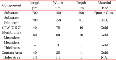
The proposed switch is designed in a generic CAD environment and the dimensions and materials used to design the switch are given in Table 1. The area of the complete switch is 0.7 mm\s\up5(2). The specifications of membrane are given in Fig. 3.
[Table 1.] Switch specifications.

Switch specifications.
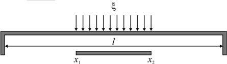
The forces act on the contact area of the membrane. As a result, the load is distributed on one-third of the area in the centre of the membrane if the load is distributed on the central component. As discussed, there is no residual stress. The force distribution on the membrane is shown in Fig. 4. Hence, the spring constant component purely depends on the force applied [14,15].
In this case, the force is distributed on both sides of the central contact, but due to that force, the central component is forced to come down in a Z direction to make complete contact with the signal line.
The force distribution can be estimated using [11]:

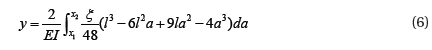
where; ξ is the load per unit of length l, I is moment of inertia and E is Young’s modulus of material. Integrating the equation (6) from x1 to x2 will give an approximation of the force distribution.
The load per unit length can be computed using:

The spring constant of the Au metal membrane is analyzed using FEM [3]. The analyzed spring constant for the membrane is 3.02 N/m. Thus, using the analyzed spring constant k, the pullin voltage can be computed and simulated. The voltage of the switch can be computed using:
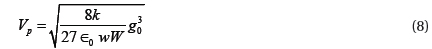
where; ε0 is the permittivity of free space, is the gap between the membrane and the electrode; wW is the area of the electrode used for actuation, w is length and W is the width of the electrode. The analytical value of the actuation voltage required for g0=3 is 16.4. Although the pull-in voltage is analyzed and compared with numerical calculations, the pull-out occurs due to the elastic recovery forces of the meanders. Hence, even for the low-k membrane, recovery forces are higher and switch stiction chances are very low.
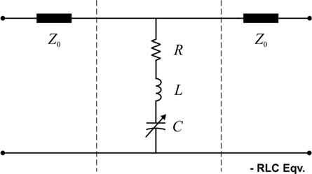
5. EQUIVALENT CIRCUIT MODELING
The equivalent circuit model of the proposed RF MEMS switch is shown in Fig. 5. The electromagnetic model for these switches can be estimated with a corresponding C-L-R circuit model. The transmission lines are terminated by characteristic impedance Z0. l is the infinite length reliant on the transmission line gap and the ohmic switch area, Cs is the series capacitance between the ohmic contact and transmission line, and Rc is the contact resistance. Two equal ohmic contact resistances Rc and capacitance Cs are considered. The parasitic capacitance between the open ends of the signal line is denoted by Cp. With the alteration in geometry of the switch, the parameters like R, L ,C or parasitic capacitance can be modified according to the performance requirements.
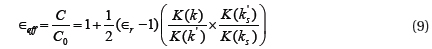
The C-L-R parametric analysis is performed for the model shown in Fig. 5. This results in capacitance of 1.38 fF and series resistance of 0.82 Ω. The dimensions of CPW are specified in Table 1. If C is the capacitance per unit length of line l and C0 is the capacitance per unit length in the absence of the dielectric layer, then the effective permittivity μeff for CPW is approximated by using:

where; K is the complete elliptical integral of the first kind, and the values of k and k' depend on the geometry configuration of the line and are demonstrated in [11].
The capacitance can be numerically computed using:
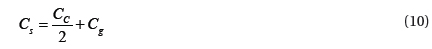
where Cg is the signal-line coupling capacitance in the OFF state due to the gap in the signal line. Cc is the contact capacitance of the switch. The series resistance (in Ω) and inductance (in pH) for the switch is calculated as 0.82 Ω and 104 pH, respectively.
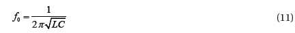
The LC resonant frequency f0 of the switch can be computed using:

where L and C are the value of inductance and capacitance.
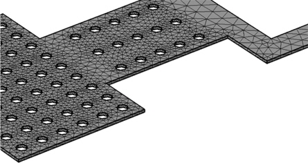
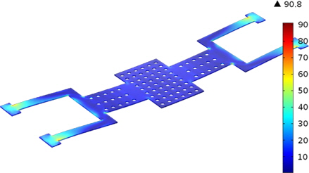
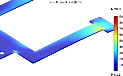
To compute the effective stress in the membrane, we have modeled the structure in the finite element modeler. Before computing the model in the FEM, meshing is required as it plays a crucial part in reducing the time of computation. The meshing of the membrane in the FEM can be seen in Fig. 6. Smaller mesh gives a more realistic solution. The effect of von Mises stress in the membrane for the required force at the specific spring constant is analyzed.
Figure 7 demonstrates that the gold membrane shows an approximate stress of 90 MPa, which is good enough for gold and less than the ultimate tensile strength of the material. That simply points to the robustness and reliability of meanders in the membrane, as this membrane can withstand many more switching cycles then the membrane made using aluminium [3,15]. This provides more room for the stress gradient. In short it can handle more stress.
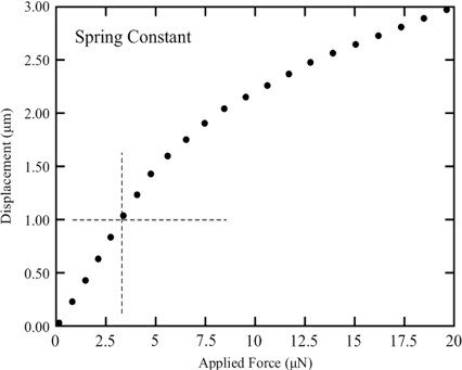
The deflection can be seen in Fig. 8 and Fig. 9 respectively. From Fig. 9, it is clear that the contact is made properly with the signal line. The spring constant is computed by applying load on the contact area of the membrane. Furthermore, the actuation voltage requirements are given in Table 2. The spring constant plot is shown in Fig. 11 and voltage requirement vs. deflection is shown in Fig. 12. The switch needs 16.4 V for the displacement of g0 as the displacement can be seen in Fig. 10.
[Table 2.] Spring constant and actuation voltage.
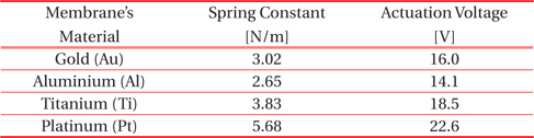
Spring constant and actuation voltage.
The spring constant and actuation voltage requirement values for different materials are given in Table. 2. The values given are simulated. The error between the measured and simulated values is minute. Hence, the simulated values are preferred. From the results, we can conclude that the use of titanium in RF MEMS switches increases the robustness and stress handling capability with a trade-off of higher actuation voltage. Titanium limits the design of low-voltage switches. As titanium is a tough material, the processes required for fabrication using this material differ to the processes that are common for fabrication using gold and aluminium.
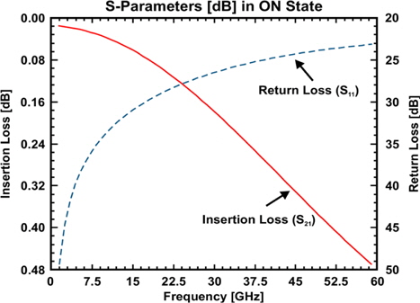
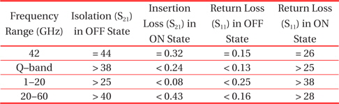
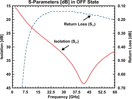
The RF performance is simulated using commercially available electromagnetic field (EM) solver, Ansys HFSS. The scattering parameters are computed for a frequency sweep of 160 for both the ON and OFF state of the switch. The proposed switch shows excellent isolation above 38 in the Q-band and a maximum peak of 2 at 42. Low insertion loss is observed as 0.32 in the Q-band and 0.05 in the X-band. S-parameters viz. isolation in the OFF state, insertion loss in the ON state and return loss in both the ON and OFF states are shown in Fig. 13 and in Fig. 14, respectively
Despite the fact that the proposed shunt RF MEMS switch results in excellent RF performance, the switch is usually optimized to maximize the switch performance until the Q-band. This switch can also be used for a higher frequency range (:>55:) with moderate RF performance. The S-parameters for both states are given in Table. 3.
[Table 3.] RF performance analysis.

RF performance analysis.
RF MEMS switches provide tremendous advantages over their semiconductor counterparts. With advancements in surface micro-machining, the proposed switch is designed/modelled using a finite element modeller and its performance evaluation and various parameters are analysed and compared with different materials. The switch is designed to overcome the most common problem of RF MEMS switches - high electrostatic actuation voltage requirements. The designed membrane has holes to overcome air the damping problem and meanders to address the high voltage requirements. Excellent RF performance, low voltage requirements, and robustness in the forefront have been analysed for this switch. The switch is optimised for Q-band operation. The proposed RF MEMS switch can potentially be used for many applications in space stations, communication networks and in systems that require low voltage.