Presently, materials like ZnO are being extensively used in optoelectronic devices, such as light-emitting diodes (LEDs), UV detectors, white light sources, and solar cells, because these materials have wide band gap (3.4 eV at 300 K) and high exciton binding energy (60 meV) [1]. However, these devices, which are fabricated using c-plane ZnO layers, have limited capacity due to spontaneous and piezoelectric polarizations caused by Stark effect [2,3]. In ZnO-based devices, the polarization-related effects can be eliminated using nonpolar a- or m-plane ZnO films. In addition, the lattice mismatches between the wurtzite structures, GaN and ZnO, are relatively small (1.9% along the c-axis direction and 0.4% along the a-axis direction [4]). Therefore, single crystal ZnO substrates can be used to grow epitaxial GaN films, with a low density of defects. However, various crystalline defects, such as dislocations and vacancies, get incorporated into the ZnO layer while growing bulk ZnO. These impurities and/or defects affect the crystallinity of subsequent epitaxial films, which are grown on ZnO substrates. In order to construct high-quality films from ZnO substrates and to improve the performance of ZnO-based devices, we need to thoroughly elucidate the electrical properties of bulk ZnO single crystals.
To accurately determine Schottky contact, we need to meticulously understand the process that governs the current flow over the Schottky barrier when a bias voltage is applied to the junction. In the presence of interface states, the flow of electric current can get impaired. Moreover, they can also adversely affect the recombination processes of carriers when the device is in operation. These interface states can be generated from surface termination, surface contamination, surface treatment, and metallization processes. Although the electrical characterization of Schottky junction can be carried out at room temperature, the low-temperature electrical characterization gives us comprehensive information about the conduction process, the nature of barrier formed at the metal-semiconductor (MS) interface, and the interface states.
In order to understand the nature of the barrier and the transport mechanism, thermionic emission (TE) theory is generally used. Using TE theory, we can determine the electrical parameters of Schottky diodes over a wide range of temperatures. In this approach, we evaluate the quality of Schottky diode by determining the ideality factor (n). Moreover, we also observe how closely the ideality factor approaches the value 1. Many previous studies have been conducted to investigate the temperature-dependent electrical properties of metal/ZnO Schottky junctions. These studies have also reported about the non-ideality of Schottky diode ( n > 1), which is formed due to the non-homogenous Schottky barrier [5-8]. However, these studies did not provide the detailed mechanisms governing current transport at different bias voltages. By considering various transport models for Pt/nGaN Schottky diodes, Suzue et al. proposed the current transport mechanisms responsible for electrical conduction at different voltages and temperatures [9]. Yan et al. have considered various transport models to analyze the experimental current-voltage (I-V) data in Ni/Au-AlGaN/GaN Schottky diodes [10]. Benmaza et al. have used various transport mechanisms to explain the I-V anomalies observed in Ni/6H-SiC Schottky diodes, especially at low bias voltage [11]. However, previous studies have not been able to elucidate the mechanisms through which electrical current conduction occurs in metal/bulk ZnO Schottky contacts. In this study, we focused on comparing the current transport mechanisms and related properties of Ag Schottky contacts in O-polar and non-polar m-plane bulk ZnO. They were measured at 300, 200, and 100 K in order to understand the different aspects of a current transport mechanism.
In this experiment, unintentionally-doped, hydrothermally-grown, O-polar (000) and m-plane (100) bulk ZnO single crystals were purchased from Tokyo Denpa Ltd (Tokyo, Japan). They were used as starting materials in the experiment. The wafers were 10 × 10 × 0.5 mm3 in dimension; they had been polished on the both the sides by the manufacturer. At room temperature, the carrier concentrations were about 5 × 1014 cm−3 according to Halleffect assessments. Before metallization, both the samples were ultrasonically cleaned using organic solvents. Silver Schottky contacts, which were 50 nm in thickness, were deposited on one side of the samples by performing radio-frequency (RF) magnetron sputtering through a shadow mask. For ohmic contact, indium metal was rubbed on the entire back surface. Currentvoltage (I-V) measurements were carried out at 300, 200, and 100 K using a HP 4156B semiconductor parameter analyzer and a cryogenic probe station (Janis ST-500).
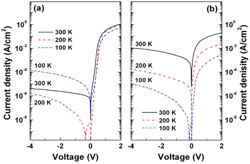
Figure 1 shows the semi-logarithmic I-V curves, which were obtained at 300, 200, and 100 K. Both the diodes revealed rectifying characteristics at all temperatures. The bias current values increased when the temperature of m-plane ZnO was increased; however, there was no increase in bias current values when the temperature of O-polar ZnO was increased. Schmidt et al. have observed that bulk ZnO, which is highly resitive in air, can be reversibly transformed into a highly conducting state under vacuum. They have reported that such behavior in the presence of an electron conducting surface channel at ZnO surface [12]. This conductive accumulation layer is compensated by acceptor-like adsorbates, such as O2 and H2O in ambient air. Furthermore, the surface conductivity increases due to the removal of some O2 and H2O adsorbates from the surface under vacuum [13]. The result indicates that regardless of the temperature, surface compensation occurred to varying extents due to acceptor-like adsorbates. Thus, this compensatory effect could be the cause of an abnormal temperature-dependent I-V behavior [ Fig. 1(a)].
The Schottky barrier heights (SBHs, φB) and ideality factors were determined from the forward bias I-V curves, which were based on the thermionic emission (TE) model [14]. The forward I-V analyses for O-plane ZnO revealed that φB = 0.802, 0.622, and 0.309 eV at 300, 200, and 100 K, respectively. The ideality factors for O-plane ZnO were 1.44, 1.67, and 3.94 at 300, 200, and 100 K, respectively. Likewise, the forward I-V analyses for m-plane ZnO revealed that φB = 0.582, 0.464, and 0.293 eV at 300, 200, and 100 K, respectively. The ideality factors for m-plane ZnO were 2.74, 2.83, and 3.47 at 300, 200, and 100 K, respectively. In both the samples, the barrier height (ideality factor) was found to increase (decrease) with increasing temperature. This temperature dependence is observed in real Schottky diodes, and the phenomenon has been attributed to the lateral variation of barrier heights [15]. Electrons at a low temperature can surmount the lower barrier; therefore, the current transport mechanism will be dominated by the current flowing through the lower barrier height. As the temperature increases, more electrons have sufficient energy to surmount the higher barrier. As a result, the dominant barrier height increases with an increase in temperature. Since the ideality factor exceeds unity, we attribute the phenomenon to the following five factors: (i) the presence of an interfacial native oxide layer, (ii) non-homogeneity of barrier height at the interface, (iii) fabrication-induced defects at the interface, (iv) tunneling current, (v) lowering of the Schottky barrier by the image force, and v) the generation of recombinant currents within the space charge region [16,17].
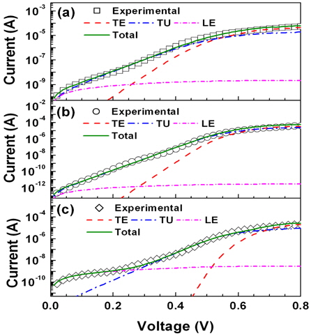
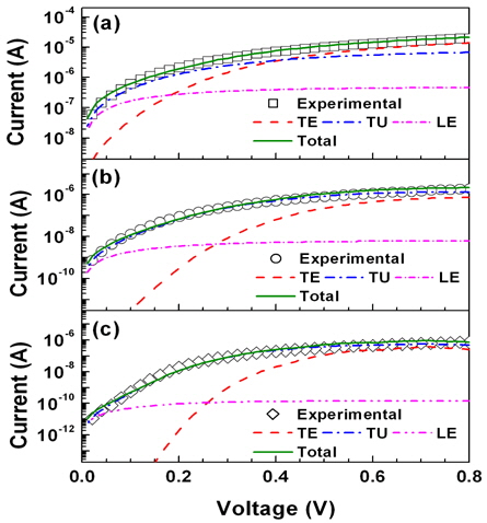
In order to elucidate the transport mechanisms in detail, other transport components were considered comprehensively. In the Schottky barrier region, a recombination current originates from the minority carrier injection. This current also contributes to the current transport. The ratio of thermionic emission to the recombination current can be estimated using the following equation: T2τ exp{q(Eg + V − 2φB) / 2 kT}[18], where τ is the lifetime of carriers; it is longer than 10−10 s in bulk ZnO [19]. The calculated ratio was >1014. Therefore, the recombination current is negligible. Then, the total current, ITOT, is assumed to be the sum of different transport mechanisms; it is calculated by the following equation [9]
where ITE is the TE current, ITU is the tunneling current, and ILE is the leakage current. The TE current is calculated using the following equation:
where ITE0 is the saturation current of the TE component, and RS is the resistance in series. Here, the ideality factor n = 1 was used to accommodate the non-ideality of I-V characteristics representing ITU and ILE. Therefore, the tunneling current is calculated using the modified equation
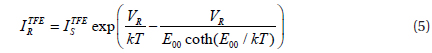
where ITU0 is the saturation current of the tunneling component. E0 = E00 coth( E00 / kT ), which is a parameter dependent on the barrier transparency; E00 = qħ / 2( Nd / meεS)1/2 is the characteristic energy related to the tunneling probability. When the applied bias voltage is sufficiently low, the leakage current can be a dominant current component, which is given by the equation:

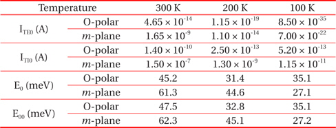
where RSh is the shunt resistance that can be approximately obtained from the reverse I-V characteristics of the diodes. The RS values were extracted from the curves in which the I-V data begin to saturate. The experimental forward bias I-V data agreed with the theoretical I-V curves in each sample, because ITE0, ITU0, and E0 were considered as fitting parameters. The experimental and fitted curves have been compared in Figs. 2 and 3, and the obtained fitting parameters are presented in table 1. At all temperatures, the TE, tunneling current, and leakage current were fitted with the experimental I-V data. The tunneling current is dominant over the entire bias region, while the contribution of TE current becomes significant in the high bias region. In particular, for O-polar ZnO at 100 K, the leakage current is dominant in the low bias region (<0.2 V). The current transport mechanism is dependent on the tunneling parameter E00, such as TE for E00/kT≪1, the thermionic field emission (TFE) for E00/kT~1, and field emission (FE) for E00/kT≫1 [20]. Table 1 presents the extracted E00 values associated with the tunneling current component. Considering the kT values (25.9, 17.2, and 0.082 meV) at 300, 200, and 100 K, respectively, we found that the E00/kT increases with decreasing temperature in both the samples. This indicates the stronger contribution of tunneling current at low temperature. This tunneling component is also associated with high ideality factors.
When thermionic field emission (TFE) or field emission (FE) model controls electric current transport, the forward bias currents can be described using Eq. (3). Then, the E00 values can be obtained from the slope of the linear regions in ln(I)-V curves, which are plotted by the ln(I)-V method. Based on this method, Das et al. calculated the E00 values for the Au/ZnO nanowire Schottky diode; the E00 values were 50 and 60 meV at 300 and 523 K, respectively. After comparing the E00 values with kT values, they concluded that the tunneling current is dominant [21]. Based on the nkT vs. kT curve (here nkT value corresponds to E0 value), Gür et al. suggested that TFE dominates the charge transport mechanism in Ag/n-ZnO Schottky diode [22]. Using ln(I)-V method, the E00 values for O-plane ZnO were found to be 40.6, 30.6, and 34.0 meV at 300, 200, and 100 K, respectively. Similarly, the E00 values for m-plane ZnO were found to be 71.4, 49.1, and 30.6 meV at 300, 200, and 100 K, respectively. In agreement with previous studies, we deduced that the tunneling current plays a significant role in the comparison of E00 values with kT values. Interestingly, the E00 values calculated by the ln(I)-V method were found to differ from those presented in table 1. Moreover, this difference becomes more significant at higher temperatures. The ln(I)-V method is applied only to the linear ln(I)-V region (the intermediate bias region). On the contrary, the fitting curves of various transport models should be matched with the experimental I-V data at low and high bias regions. In addition, the contribution of TE current to the total current probably increases with an increase in temperature. These might cause differences in E00 values. Because electrical current is a sum of different current components, we considered analyzing the I-V data using various transport models. Thus, we obtained more exact E00 values.
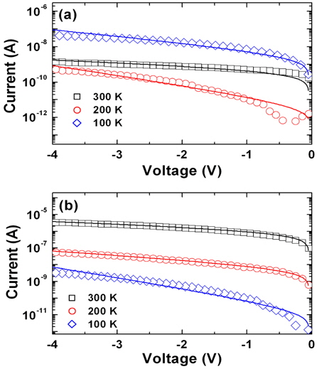
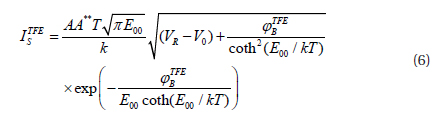
The reverse current, IR, was analyzed using TFE [23], which is expressed by the equation
and
where VR is the reverse bias; A** is the Richardson constant; V0 = kT/ q ln( NC / Nd ), which is the potential difference between the conduction band and Fermi level, and is the barrier heights for TFE model. The experimental reverse I-V data fitted with the theoretical I-V curves of each sample when E00 and were considered as fitting parameters. The comparison between experimental and fitted I-V curves is shown in Fig. 4. For O-polar ZnO, the fitting values of barrier height were found to be 0.705, 0.598, and 0.208 eV at 300, 200, and 100 K, respectively. Likewise, the fitting values of barrier height for m-plane ZnO were found to be 0.505, 0.460, and 0.273 eV at 300, 200, and 100 K, respectively. These values are smaller than those obtained from the forward bias ln(I)-V curves. Çınar et al. have observed that in Ag/p-GaN Schottky contacts, the barrier heights associated with the forward bias current are higher than those associated with the reverse bias current [24]. They proposed that at the Schottky interface, the fixed surface charge additionally ionizes doping atoms, making the width of the barrier height thinner at the surface. This facilitates the tunneling of carriers through the barrier, eventually lowering the barrier under reverse bias.
For O-polar ZnO, the fitting values of E00 were 0.01, 3.55, and 0.01 meV at 300, 200, and 100 K, respectively. For m-plane ZnO, the fitting values of E00 were 0.01, 1.35, and 1.10 meV at 300, 200, and 100 K, respectively. Since the carrier concentration was 5 × 1014 cm−3 in both the samples, the E00 value was calculated to be about 0.25 meV. The result indicates that for both samples, the electron conducting surface channel at the ZnO surface becomes passive and active at 300 and 200 K, respectively. At 100 K, O-polar ZnO becomes again resistive, whereas m-plane ZnO still remains highly conductive. The atomic force microscopy (AFM) image of O-polar ZnO showed a fairly flat surface with a root-mean-square (rms) value of ~ 0.40 nm. On the other hand, the AFM image of m-plane ZnO displayed a corrugated morphology with an rms value of ~ 0.90 nm. Such different surface morphologies and surface defects (e.g., oxygen vacancies) might affect the activation (and passivation) of acceptor-like adsorbates at low temperatures. However, further investigation must be conducted to understand the exact mechanism.
The current transport properties of Ag Schottky diodes in Opolar and non-polar m-plane bulk ZnO were measured at 300, 200, and 100 K. Then, these current transport properties were compared using considering various transport models. Since the electrical current is the sum of different current components associated with different transport mechanisms, we deduced that the analysis of I-V data should be carried out using various transport models to determine exact values of electrical parameters, such as E00 value (the characteristic energy related to the tunneling probability). The fitting of the forward bias currentvoltage (I-V) characteristics revealed that the tunneling current is dominant as the transport component in both the samples. We observed that the contribution of tunneling current became significant at low temperature, so it is responsible for higher ideality factors at low temperatures. We also found that the tunneling current was dominant over the entire bias region, except for O-polar ZnO at 100 K (in that case, the leakage current was dominant in the low bias region). Furthermore, the contribution of TE current becomes important in high bias region. Using the thermionic field emission (TFE) model, the reverse bias I-V characteristics were well fitted in both the samples. The tunneling effect is affected by the different surface morphologies and surface defects of both samples as they cause different degrees of activation/passivation of acceptor-like adsorbates.