A push-push voltage controlled dielectric resonator oscillator (VCDRO) with a modified frequency tuning structure using broadside couplers is investigated. The push-push VCDRO designed at 16 GHz is manufactured using a low temperature co-fired ceramic (LTCC) technology to reduce the circuit size. The frequency tuning structure using a broadside coupler is embedded in a layer of the A6 substrate by using the LTCC process. Experimental results show that the fundamental and third harmonics are suppressed above 15 dBc and 30 dBc, respectively, and the phase noise of push-push VCDRO is -97.5 dBc/Hz at an offset frequency of 100 kHz from the carrier. The proposed frequency tuning structure has a tuning range of 4.46 MHz over a control voltage of 1–11 V. This push-push VCDRO has a miniature size of 15 mm×15 mm. The proposed design and fabrication techniques for a push-push oscillator seem to be applicable in many space and commercial VCDRO products.
Microwave circuit technologies have been rapidly enhanced along with commercial wireless communication development. The circuits are becoming increasingly small and compact. Further, signal sources in communication systems require high reliability, good stability, low cost, and low phase noise performance.
The three-dimensional integration capability of the low temperature co-fired ceramic (LTCC) technology can lead to circuit size reduction and low-cost design. At the same time, a small value of the dielectric loss tangent reveals excellent high-frequency characteristics. Therefore, LTCC technologies are widely attracting the attention of microwave and millimeter-wave engineers because of their superior advantages over other substrate technologies [1-3].
A dielectric resonator (DR) has many advantages in terms of size and quality factor (Q-factor) over stripline resonators and waveguide cavities. Further, a dielectric resonator oscillator (DRO) is a cost-effective solution for achieving a highly stable and low-phase noise source in the microwave and millimeter-wave range [4]. In general, a highly stable signal source is achieved by phase locked loop in order to meet the above mentioned conditions [5].
Voltage controlled oscillator is necessary for a phase locked source, and it is not easy to realize the frequency tuning circuit in push-push-type oscillators. The push-pushtype oscillator theory has been published in many papers [6-8]. In this paper, a modified frequency tuning circuit using broadside couplers is adopted in push-push DRO by using the LTCC technology.
II. LTCC DIELECTRIC RESONATOR OSCILLATOR DESIGN
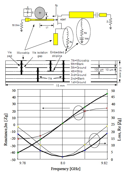
In DRO configurations, a popular design topology is the series feedback type and the transistor is self-biased with the resistor connected to the source of the high electron mobility transistor (HEMT). An FHX35X chip HEMT provided by Fujitsu is used as an active device for DRO. The DRO is designed and fabricated with the LTCC process of the Ferro A6 substrate, which has six dielectric layers. The relative permittivity (
Fig. 1 illustrates the configuration of the LTCC DRO. The first and the fifth metal layers are used for grounding. The drain and source bias circuits for HEMT are embedded in the third metal layer. The coupling line with DR is located at the gate port along with a positive feedback microstrip line at the source port and a drain matching circuit at the seventh metal layer. The second, fourth, and sixth metal layers are blanked by considering the LTCC fabrication process under the condition of minimum line width and gap between the microstrip lines. A dielectric thickness of more than 100 µm leads to the implementation of a high impedance transmission line.
Fig. 1 also describes the DR coupled with the microstrip line, and Z
III. FREQUENCY TUNING CIRCUIT DESIGN IN LTCC PUSH-PUSH DRO
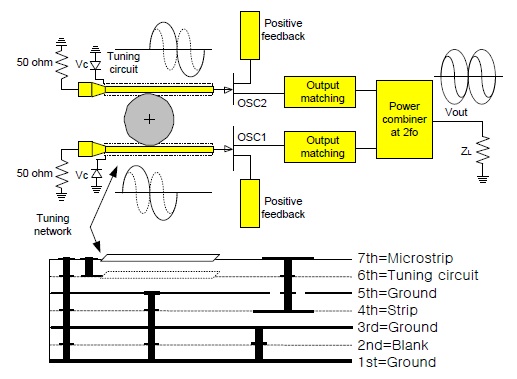
Fig. 2 shows the configuration of LTCC push-push VCDRO. The series feedback-type oscillator is suitable for the implementation of the push-push oscillator with DR due to the TE01δ mode electromagnetic field. In this study, the push-push VCDRO consists of two series feedbacktype oscillators, a Wilkinson power combiner at 2fo, and a frequency tuning circuit using broadside couplers. The DR is placed between parallel microstrip lines and coupled with the respective microstrip lines of OSC1 and OSC2 simultaneously. The gate current of HEMT in OSC1 is 180° out of phase compared to that in OSC2 at the odd-mode harmonics, and is in-phase at the even-mode harmonic. Symmetrical OSC1 and OSC2 generate signals at the half output frequency as follows:


Except for the phase difference of

The push-push oscillator gives only even-mode signals in the case of perfectly symmetric OSC1 and OSC2 [8].
Fig. 2 also illustrates a resonant frequency tuning structure with broadside couplers and varactor diodes. In general, it is difficult to insert a tuning circuit into a planar push-push oscillator.
However, in this study, one side of a broadside coupler presented as a solid transmission line used as a transmission line coupled with DR, and the other side presented as a dashed transmission line used for the frequency tuning circuit. The other side of the broadside coupler is embedded in the sixth metal layer, which is blanked in the LTCC process. The dashed transmission line for tuning DR has a half wavelength, and the DR is placed at the center of the dashed transmission line for maximum magnetic coupling.
The manufactured push-push VCDRO based on the LTCC process is oscillated around 16 GHz, and the position of the DR is fixed approximately at the vicinity of a quarter-wavelength from the gates of the transistors. The output spectrum and phase noise characteristics are measured using the Agilent-8565E spectrum analyzer.
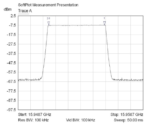
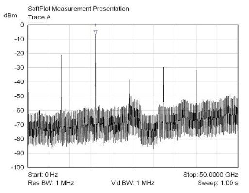
Fig. 3 shows the full span spectrum of the 8565E analyzer. The output power is -6.83 dBm. The fundamental and the third harmonic suppression are measured to be about 15 dBc and 30 dBc, respectively.
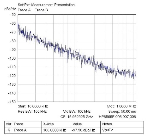
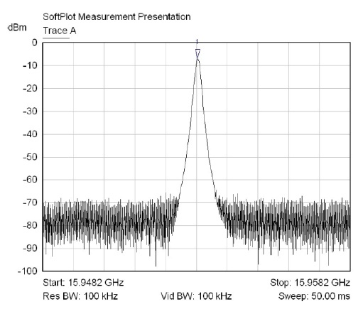
Fig. 4 presents the output power of -6.83 dBm, including a cable loss of about 2.0 dB. The center frequency is measured to be a little lower than the target frequency, but the center frequency can be adjusted to 16 GHz accurately by slightly adjusting a tuning screw. The proposed pushpush VCDRO shows the phase noise characteristics of -97.5 dBc/Hz (marker1) and -120 dBc/Hz at the offset frequencies of 100 kHz and 1 MHz from the carrier, respectively, as shown in Fig. 5.
Fig. 6 shows the tuning range of 4.46 MHz over the control voltage of 1–11 V for varactor diodes in the proposed tuning structure. The flatness of the tuning range is within ±0.1 dBm. This tuning range characteristic exhibits a good performance in the implementation of a phase locked oscillator.
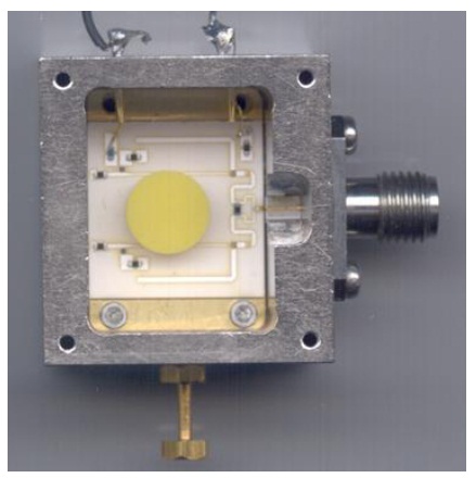
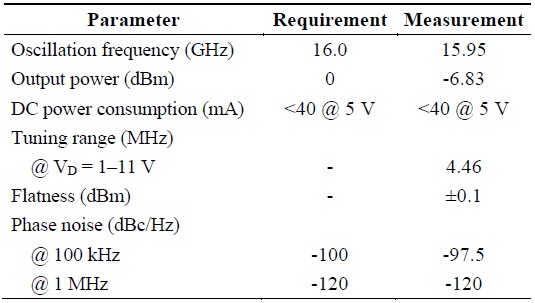
Fig. 7 shows a photograph of a miniature push-push VCDRO with the circuit measuring 15 mm×15 mm. The performance of the manufactured push-push VCDRO is summarized in Table 1. The output power and the phase noise at an offset frequency of 100 kHz are a bit short compared to the requirements. However, these characteristics can be overcome by the buffer amplifier and the loop bandwidth of the phase locked loop system.
The electrical performance of the developed push-push VCDRO with the proposed tuning structure
A push-push VCDRO using the LTCC technology based on a Ferro A6 substrate having a dielectric thickness of 100 µm and metal thickness of 10 µm has been demonstrated. The frequency tuning structure using a broadside coupler of this push-push VCDRO is embedded into a layer of the A6 substrate. The push-push VCDRO shows fundamental and the third harmonics suppression of 15 dBc and 30 dBc without a band pass filter, and the tuning range is 4.46 MHz over the control voltage of 1–11 V within ±0.1 dBm. The phase noise is measured to be -97.5 dBc/Hz at an offset frequency of 100 kHz from the carrier. This push-push VCDRO can be applied in a phase locked environment. Further, the proposed design and fabrication techniques for a push-push oscillator seem to be applicable in many space and commercial products such as the Ka-band satellite receiver, wireless LAN, and mobile communication systems.