We report a numerical analysis of the light-extraction efficiency (LEE) of light-emitting diodes (LEDs) on patterned sapphire substrates (PSSs). We considered various n-sided, regular convex pyramids, where n is an integer and n ≥ 3. We then considered four cross sections: extruded, subtracted, truncated-extruded, and truncated-subtracted. Ray-tracing simulations were carried out with these polygonal pyramid patterns, and the dimensions of the patterns were systematically varied. Optimized pattern shapes were determined for large LEE. An extruded circular pyramid with a slant angle of 45° was found to be the optimal patterned shape.
Light-emitting diodes (LEDs) are solid-state light sources that exploit electroluminescence in semiconductor materials to generate light. LEDs are semiconductor
The light-extraction efficiency (LEE) of LEDs is an important parameter. The LEE of an LED is defined as the ratio of the number of photons emitted into free space from an LED chip to the number of photons emitted from the active region inside the LED chip [1]. It is limited by total internal reflection (TIR) inside the LED semiconductor chip, which typically has a larger refractive index than the surrounding material. When the light generated from the active region inside the semiconductor is incident upon the interface between the semiconductor and the surrounding space, if the angle of the emitted light exceeds the critical angle, TIR occurs and light is trapped inside the semiconductor, eventually being dissipated as heat. The LEE of an LED is typically small, because there is a large difference in refractive index between the semiconductor and the surrounding space [2]. For example, the refractive index of gallium nitride (GaN) is 2.5, and the LEE of a GaN-based LED chip with a simple rectangular shape into free space is only 4% [1, 2]. Numerous approaches have been used to improve the LEE, including photon recycling [3], flip-chip configurations [4], resonant cavities [5], a transparent surface contact layer [6], sidewall treatment [7], surface roughening [8], photonic crystals [9], chip shaping [10], and patterned sapphire substrates (PSSs) [11-14]. PSSs employ arrayed patterns on the entire top surface of the sapphire that forms the LED substrate. Scattering and multiple reflection of the light inside the LED chip can be enhanced with these structures, breaking the TIR condition and therefore improving the LEE. The PSS can also serve to reduce the threading-dislocation density during the growth of LED epitaxial layers.
Monte Carlo ray-tracing simulations are one of the most popular optical simulation methods for the analysis of photonic devices [15-18]. Geometrical optical phenomena in photonic devices can be analyzed using this method, including ray scattering, absorption and transmission in the semiconductor layers, Fresnel losses of the media due to different refractive indices, and the randomly emitted light from the active region of an LED [19]. Although a number of studies of the numerical design of PSSs have been reported, a systematic study of
Here we describe numerical simulations for LEDs using the Monte Carlo ray-tracing method. We examined the LEE of LEDs using PSSs, focusing on PSSs with various polygonal pyramid patterns. By systematically varying the possible shapes of the polygonal pyramid patterns, we determined the pattern shape and size for optimal LEE.
II. RAY-TRACING SIMULATION PROCEDURES
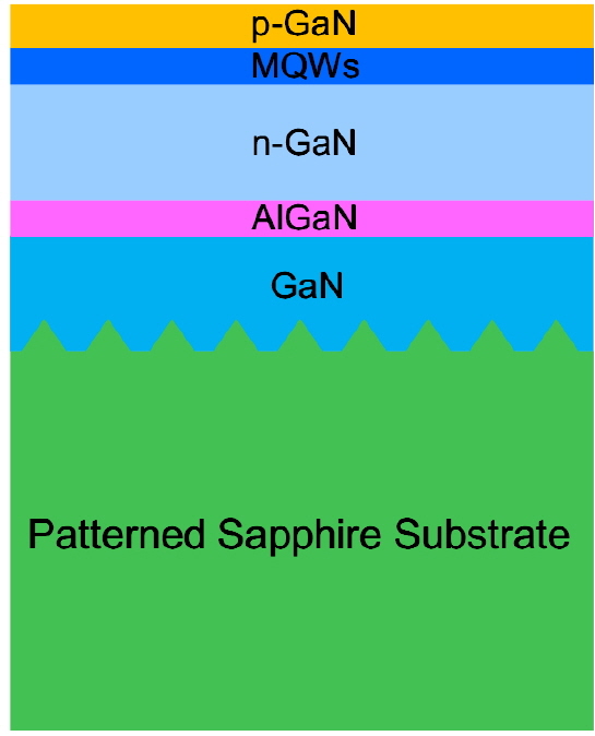
We used the software application LightTools to implement ray-tracing simulations. Figure 1 shows a schematic diagram of the simulated GaN-based PSS-LED structure. The size of the chip was 300 × 300 μm2. The parameters for each layer in the PSS-LED structure are listed in Table 1. The device consisted of a 330-μm-thick sapphire substrate, a 2-μm-thick GaN layer, a 0.05-μm-thick (Al,Ga)N layer, a 2-μm-thick
[TABLE 1.] Parameters for each layer in the ray-tracing simulations of the PSS-LEDs
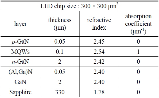
Parameters for each layer in the ray-tracing simulations of the PSS-LEDs
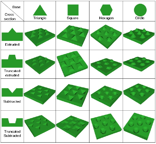
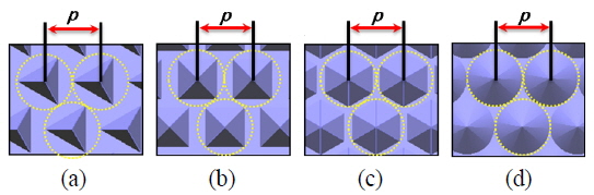
We chose to consider only polygonal pyramid patterns, because these patterns can be expected to be fabricated reasonably on the sapphire substrate via simple control of the 2D etching mask pattern shape, in addition to the etching conditions. We did not consider pillars because the slant angle of the pillar pattern is fixed at 90°, and so trapped light cannot efficiently out-couple via multiple reflections.
We aimed to cover many possible shapes of the polygonal pyramid patterns. We considered pyramids with bases of
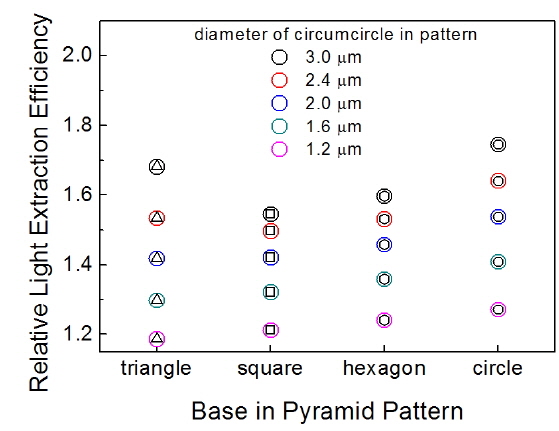
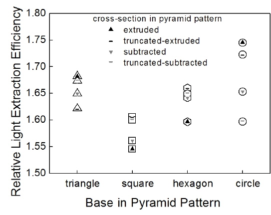
Figure 4 shows simulated relative LEEs of the PSS-LEDs with various polygonal pyramid patterns. We started with a pitch of
For each base shape, with a fixed pattern pitch, the LEE increased with the circumcircle diameter. In other words, the LEE increased as the fraction of the patterned surface area increased, and reached a maximum when the circumcircle diameter was at its maximum, i.e.
With a fixed circumcircle diameter, the circular-base pyramid exhibited a larger LEE than those with
Four cross-sectional shapes were considered: extruded, subtracted, truncated-extruded, and truncated-subtracted. We fixed the pattern pitch at
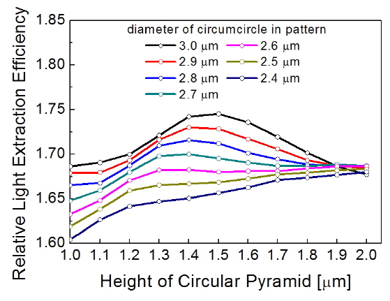
After determining the optimal geometry of the base and the cross section of the pyramid, we varied the vertical height, thereby varying the slant angle. Figure 6 shows the LEE with the extruded circular-base pyramid patterns as a function of pattern height, for various diameters of circumcircles with a pitch of 3.0 μm. For a given height of the pattern, the LEE increased with the diameter of the circumcircle. For a given circumcircle diameter, when
Based on these results, we can conclude that the extruded cross section and circular-base pyramid pattern with
Additionally, we want to make the following points regarding the basic concern about the validity of the ray-tracing model for the calculation of LEE in PSS-LEDs with micron-sized structures. It is known that most researchers have successfully simulated light extraction in LEDs using the ray-tracing method when they considered LEDs with mixed structure sizes, i.e. some micron-sized structures and some submicron-sized, like our LEDs [14, 16, 17, 19, 20], even though they used a strict method such as the finite-difference time-domain (FDTD) method when they considered LEDs with entirely nanoscale structures. The validity for such a use of the ray-tracing method can be explained: The key point in the phenomenon of light extraction with PSS-LEDs is the breaking of TIR, so that the light’s nature as a ray is more conspicuously considered than as a wave. Recently, it has also been reported that simulation results for LEE enhancement of LEDs with entirely nanoscale structures are similar for ray-tracing and FDTD, the difference not exceeding 8.5% [18], which justifies our reasoning above.
We have described the results of Monte Carlo ray-tracing simulations of the LEE of PSS-LEDs with various polygonal pyramid patterns. We systematically varied the geometry of the polygonal pyramid patterns, and found relationships between the LEE of PSS-LEDs and the geometry of the patterns. The LEE increased as the fraction of the unpatterned planar surface area decreased. Triangular- and circular-base pyramids yielded a maximal LEE for an extruded cross section, whereas square- and hexagonal-bases had maximal LEEs for a truncated-extruded cross section. The LEE was largest for a circular base, followed by a triangular base. In general, the LEE increased with the height of the pattern when there was a large fraction of unpatterned planar surface. However, when the fraction of the unpatterned planar surface was below a certain critical value, the pattern exhibited an optimum height. The circular-base pyramid pattern with an extruded cross section,