We fabricated a periodically poled lithium niobate (PPLN) by direct laser-writing of a quasi-phase-matching (QPM) structure in photolithographic process. Because we do not need to prepare a photomask by electron-beam writing, the “maskless” process shortens the fabrication time and significantly reduces the cost. We evaluated the poling quality of the direct laser-written PPLN by measuring the diffraction noise from the surface relief pattern of the fabricated QPM grating and comparing the results to those from a conventional PPLN made with a photomask. The quality of the PPLN fabricated by direct laser-writing was shown to be equivalent to that fabricated by the conventional method.
Quasi-phase-matching (QPM) has been applied to ferroelectric crystals for efficient nonlinear frequency conversion such as second-harmonic generation and optical parametric generation/oscillation. Although ferroelectric crystals such as LiNbO3 and LiTaO3 have intrinsically large nonlinear coefficients (
A conventional fabrication process of a representative QPM device, a periodically poled lithium niobate (PPLN) crystal, can be summarized as follows: (1) making a photomask with a designed electrode pattern (typically with a well-defined QPM period) by electron-beam writing on a metal-coated fused silica plate, (2) preparing a thick photoresist (PR) layer on the positive z-face of a LiNbO3 wafer, (3) exposing a UV-light through the photomask in contact with the PR-layer, (4) forming the patterned electrodes by developing (washing out the exposed PR area), and finally (5) high-voltage poling in an electrolyte. Additionally, metal electrodes can replace the liquid electrodes between steps (4) and (5). Among the typical PLP steps of (1)~(4), the electron-beam writing [step (1)] is a costly process and takes a lot of time in most optics laboratories. Reducing the fabrication time is also desirable for obtaining efficient feedback between the design and the fabrication process steps.
Direct writing of the electrode pattern by scanning of a focused laser beam can result in a faster turnaround time and be more economical, because the manufacturing process of a photomask can be omitted [3-7]. An advantage of this “maskless” process is that the nonlinear optical properties can be tailored by modifying the structure of the ferroelectric domains more easily and quickly. However, it can also generate some problems such as decreased period stability and increased duty cycle error due to the limited quality of the laser beam scan. In this work, we fabricated a maskless PPLN crystal, and assessed the poling quality by the diffraction method reported in our previous work [8]. The poling quality of the maskless PPLN was proven to be equivalent in terms of period stability and duty cycle error to that of conventional PPLN fabrication using a photomask.
II. FABRICATION PROCESSS FOR MASKLESS PPLN
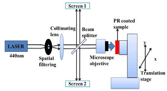
A schematic set up for our direct laser-writing system is shown in Fig. 1. The positive face of a congruent z-cut LiNbO3 (LN) plate (5 mm thick, Crystal Technology) was coated with a PR (Clariant, AZ5214E type), forming a 2 μm thick PR-layer as in the conventional poling process using a photomask. This thick PR layer is necessary because it acts as an insulator, and provides a difference in the electric fields applied to the PR region and the bare LN surface, which should be lower and higher than the coercive field, respectively. After thoroughly drying the PR-coating, the plate was mounted on a computer-controlled x-y translation stage.
The laser source was a 440 nm wavelength laser diode module (World Star Tech, Canada). We first tried a wavelength of 405 nm at which the PR layer has much stronger absorption than at 440 nm. However, most light was absorbed only near the surface, and the deep region of the PR layer, closest to the lithium niobate surface, was not sufficiently exposed. Thus, we selected a 440 nm laser for deeper penetration into the PR layer, with moderate absorption throughout the thickness. The laser beam was spatially filtered to have a near-Gaussian distribution, collimated, and focused on the PR-layer with a microscope objective lens, making a spot size of 13 μm in diameter, with the goal of writing a grating with a period of 27 μm (37 lines/mm). It took about 6 minutes to scan an area of a 15 mm-long (y-direction) and 1 mm-wide (x-direction) grating.
If the laser beam was more tightly focused, the scanning time would be reduced and finer lines could be written. However, a smaller beam waist results in a smaller Rayleigh range, making it difficult to keep the PR-layer within this range throughout the scanning process. If the sample gets out of the focus range during scanning, non-uniform exposure takes place, which can result in under/over-developed regions or non-parallel grooves. Focus calibration of the translation stage was done by comparing the images of the incident beam (on screen-1) and the reflected beam (on screen-2) while a mirror with the same thickness as the sample was placed on the sample stage during a test scan. Then the PR-coated sample was mounted on the stage at the mirror position. This method allowed us to keep the sample within the Rayleigh range (0.6 mm) during scanning. It should be noted that the PR-layer thickness is negligible compared to the Rayleigh range.
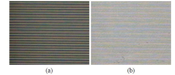
After scanning, the exposed PR regions were washed out in a developer solution, and dried to form a PR-grating, as shown in Fig. 2(a). A good PR-grating should have a significant depth (2 μm here) and clear bottom edges touching the surface of the LN plate. In order to obtain a successful poling result, it is important not to leave any residual PR, revealing the bare surface of LN at the electrode sites. A laser power of 0.32 mW was found to be optimum under the experimental conditions specified above. The developed sample was brought into the standard high-voltage poling process, where liquid electrodes were used [9]. After poling, it was cleaned with ethanol to remove the PR layer, and the opposite side (the negative z-face) was etched slightly in an acid to reveal the surface relief grating structure and visually check the overall uniformity of the QPM structure (Fig. 2(b)).
III. POLING QUALITY EVALUATION METHOD
For the optimal performance of a QPM device, the ferroelectric domain structure after poling must ensure good fidelity to the designed grating structure. However, local deviations from the ideal domain-wall locations occur statistically during the poling process, which can lead to decreased efficiency or undesired device function such as parasitic harmonic generation [10]. However, for a QPM device with reasonably good quality, visible defects such as domain merging are rarely observed, and the poling quality is not easily compared quantitatively with QPM devices fabricated by different processes. For such devices, the two major factors affecting the final device performance are period stability and random duty cycle (RDC) error [1, 10, 11].
In our laser-writing system, since the y-axis motion controlled by a stepping motor defines the spacing between the successive grooves, the accuracy of the stepping translation determines the period stability. RDC error is another concern for the maskless PPLN. The laser-written PR-grating may have delicate differences in shape from the conventional grating created by contact UV exposure through a photomask, which can lead to different statistics in the formation of the reversed domains in the poling process.
To check the quality of fabricated QPM devices, several methods have been proposed that examine the periodically poled domain structure [12-19]. Some methods are based on diffraction experiments [9, 20, 21]. In these works the duty cycle information was obtained by analyzing the diffraction patterns from etched surface-relief pattern or index modulation that was built in to the periodically poled crystals. Recently, we proposed simple yet powerful diffraction methods [8, 22] to quantify the statistical information about RDC error. For this method, period stability can be easily checked by comparing the widths of the diffraction orders against those calculated by theory. Here, the poling quality of our fabricated maskless PPLN was evaluated by the diffraction-noise method [8], the result of which is summarized below.
When a uniform beam illuminates a grating with

where
IV. DIFFRACTION NOISE MEASUREMENT
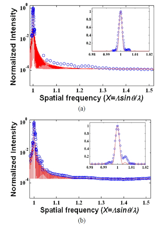
A surface-etched grating area of 10 mm × 1 mm was uniformly illuminated by a He-Ne laser beam expanded and collimated in one dimension (grating vector direction), and the far-field diffraction intensity pattern was measured as detailed in [8] and [22]. Here, the number of periods under illumination was
We also compared the poling quality by comparing the diffraction noise of the maskless PPLN with a conventional PPLN made using a photomask, as shown in Fig. 3(b) [22]. For the conventional PPLN, the RDC error was estimated as
Also shown in the insets of Figs. 3 (a) and (b) are expanded views of the first orders diffraction peaks. The fact that they fit well to the calculated curves confirms that the maskless PPLN also has as excellent period stability as the conventional PPLN. The broader first order peak in Fig. 3(b) than in (a) is again due to the smaller period numbers in (b).
We fabricated a PPLN by a direct laser-writing technique and evaluated the poling quality by a diffraction noise measurement. From the results, we can conclude that the maskless PPLN has equivalent poling quality to the conventional PPLNs fabricated with photomasks. The direct laser-writing technique provides a cost-effective and flexible alternative to the conventional fabrication process involving a photomask. We also demonstrated that, combined with the direct laser-writing fabrication, the simple diffraction method [8] provides a fast feedback to the newly developed poling processes, and helps improving the fabrication conditions quickly, and the overall poling quality of the devices as a result.