Optical spectrometers have a long history from early human civilization to today. Their key characteristic of spectral-to-spatial mapping is widely applicable in chemical and biological fields. Recently, it has become very important to reduce size and integrate devices in order to construct a lab-on-a-chip device. However, the primitive grating-based-spectrometers should have large enough size to support diffraction and imaging of light, thus they have an intrinsic limit to miniaturizing their operating size [1-4]. Many studies of the spectrometer with micrometer scale [5-9] have come out recently, while the sub-micrometer region is still a challenge to design and operate.
Plasmonic channel-waveguide, which can be designed as a sub-micrometer cavity to apply to a nanolaser [10, 11] or a refractive index sensor [12], has been studied in recent years. The dispersion curve of the square channel-waveguide has a cutoff frequency, and adjacent two channel-waveguides with different widths make a mode gap since the cutoff frequency shifts depending on the waveguide width. Cutoff frequency increases by decreasing the width, thus the narrower waveguide acts as a mirror. The previous studies used this mechanism to build a Fabry-Perot cavity by placing two narrow waveguides to both the left and the right of a broader square channel-waveguide cavity. The structures achieved a compact photon confinement with only a few hundred nanometers size, including the cavity and side waveguides [11, 12].
In this study, we propose a plasmonic tapered channel-waveguide structure as a sub-micrometer-sized spectrometer. This spectrometer uses the cutoff mechanism to control a scattering point depending on the wavelength, which is able to perform spectral-to-spatial mapping by observing the movement of that point. The tapered channel-waveguide structure is an on-chip structure with a physical size of 0.24×2.0×0.20 μm3. We used the finite-difference time-domain (FDTD) method to investigate the characteristics of the tapered spectrometer. We will discuss the scattering behaviors in the proposed structure for different incident wavelengths.
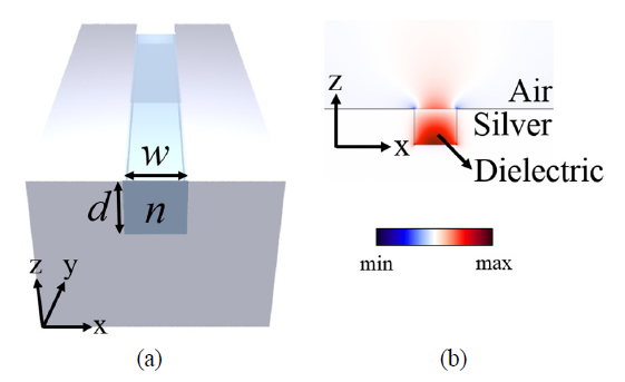
2.1. Plasmonic Square Channel-waveguide
Our spectrometer is based on a plasmonic square channel-waveguide with width of
2.2. Dispersion Property and Cutoff Frequency
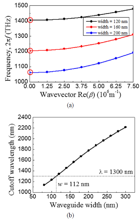
We investigated frequency dependencies of the channel-waveguide mode on the waveguide width. Figure 2(a) shows the dispersion relations of the channel-waveguide mode for different widths of 120 nm (black), 160 nm (red), and 200 nm (blue). The curves move to lower frequency region for larger waveguide width. This is because field cross-section increases when the waveguide width increases.
In this plasmonic square channel-waveguide, there exist cutoff frequencies at the wave vector of zero, indicated by red circles in Fig. 2(a). The cutoff frequency for the waveguide with
Figure 2(b) is a plot of cutoff wavelength as a function of the waveguide width. At the waveguide width of 80 nm, the cutoff wavelength is 1135 nm, and at the width of 300 nm, the cutoff wavelength becomes 2216 nm. Cutoff wavelength linearly increases by increasing waveguide width. When the incident wavelength is assumed to be 1300 nm, the cutoff width is estimated to be 112 nm.
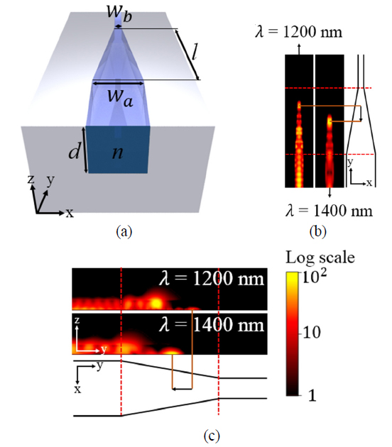
3.1. Plasmonic Tapered Channel-waveguide
We designed a tapered channel-waveguide consisting of two widths, an entrance width,
Figure 3(b), (c) shows propagation and reflections at the tapered region for the SPP waves with wavelengths of 1200 nm and 1400 nm in the waveguide. Here, the time averaged |E|2 field images are represented as log scale at the x-y plane (b) and the y-z plane (c). The tapered structure at right (b) and below (c) the electric field intensity images indicates how the reflection point changes depending on the source wavelength. The reflection points are 1460 nm for λ = 1200 nm and 1040 nm for λ = 1400 nm from the starting point of the tapered region. As shown in Fig. 3(b) and (c), the source with shorter wavelength propagates more than that with longer wavelength. This wavelength dependent SPP propagation can be applied to spatial mapping of the spectrum, which allows the tapered waveguide to act as a spectrometer.
3.2. Detection of the Scattering Wave
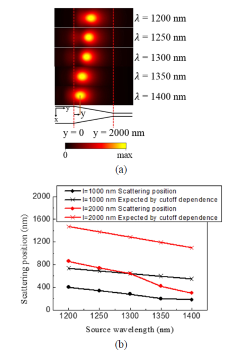
As a practical matter, it is hard to observe the movement of the reflection point at the bottom of the narrow waveguide. However, the open-cell structure of the proposed channel-waveguide allows the SPP wave to scatter at the reflection point, and the scattered wave moves depending on the reflection point. This scattered wave can easily be detected and mapped by the camera as an intensity distribution in the x-y plane. For this reason, we investigated time averaged up-going Poynting vector (Sz) images in the x-y plane at height
Figure 4(b) is a plot of the scattering position versus source wavelength from 1200 nm to 1400 nm for different tapered spectrometer with
In Fig. 4(b), the slope of the graph, which indicates spatial distribution of the different wavelengths, strongly depends on the tapered length
We proposed a plasmonic tapered square channel-waveguide as a sub-micrometer-sized spectrometer. The tapered channel-waveguide can map the spectrum image by spectral-to-spatial dependent scattering wave, based on cutoff wavelength mechanism. We investigated the dispersion curves of the channel-waveguide with several waveguide widths, and the cutoff wavelength dependences on the waveguide width, to analyze and expect the characteristics of this type of spectrometer. The cutoff wavelength shows linear dependency on the waveguide width. We applied the width dependence to design tapered channel-waveguide, and used the cutoff mechanism to control the scattering position which indicates the wavelength of the incident light. Also, in order to provide a practical measurement scheme, we calculated vertical Poynting vector images of the up-going scattering wave upper the waveguide top. The single, localized bright spot that occurred in the images moved linearly by change of the source wavelength. Therefore, since the spot position has spectral dependence, one can map the spectrum of the incident light to spatial intensity distribution. As a result of the calculation, the spot moved clearly for the wavelength difference of 50 nm. In addition, for the tapered length of 2000 nm, the wavelength change of 200 nm from 1200 nm to 1400 nm results in the large scattering spot movement of Δy = 560 nm. In addition, our spectrometer takes on-chip structure with a physical size of 0.24×2.0×0.20 μm3.