An optical grating can be encoded on a sample surface by two-beam interference using a single near-infrared femto-second laser pulse [1, 2]. Diffraction gratings have been commonly fabricated on silver halide emulsion, photoresist, and photopolymer optical materials, for example [3-5]. With individual femtosecond laser pulses, permanent gratings have been encoded on surfaces of glass, crystal, and silicon dioxide thin film [6-9]. The fabricated surface-relief or refractive-index gratings can be applied for holographic data storage, diffractive optics, and optical information processing.
Among transition metal oxides, those of niobium, tantalum, or titanium are recognized as preferred candidate materials for waveguiding layers on optical (grating-coupler) waveguides, due to their high optical transparency, high index of refraction, ultrafast optical response, and chemical and thermal stability [9]. In particular, aluminum oxide materials prepared via atomic layer deposition (ALD) have been used successfully for high-efficiency diffraction gratings. ALD is a cyclic process involving sequential, self-limiting surface reactions. During ALD a volatile precursor (typically a metal-organic molecule) and a co-reactant (typically an oxidizing or reducing agent) are delivered in a time sequence, and isolated from each other in an inert-gas purging step [10]. ALD has been widely used in microelectronics and has found various other applications in the past several decades [11]; however, it is relatively new and is emerging as an important method for electrochemical devices and processes. Dielectric films grown using the ALD method exhibit higher refractive index and molecular density than films grown using other deposition methods. For instance, the fabrication and characterization of waveguide gratings on the surface of titanium oxide (also deposited using an ALD device) indicated inorganic materials with both high refractive index and high dielectric constant [12, 13]. Recently, ALD has emerged as a thin-film deposition technique yielding exceptional film uniformity and conformity, and precise thickness control [14].
In this study, the fabrication of microscale holographic gratings on an Al2O3 surface using a femtosecond laser pulse was demonstrated. A holographic grating using a two-beam interference method on Al2O3, deposited using an ALD device, has never been reported. Common methods to fabricate gratings on dielectric materials including electron-beam lithography and ion etching [15, 16], but these methods are time-consuming and costly. Using the holographic grating method, the fabrication time and cost can be reduced.
Analytical and graphical profiles based on Kogelnik’s coupled-wave theory [17] provide a vivid description of the simple sinusoidal grating. The thicknesses and characteristics of the samples were observed using a scanning electron microscope (SEM).
Aluminum oxide deposited on a silicon wafer and indium tin oxide (ITO) glass were selected as the sample materials. Compared to other materials, such as a polymethyl methacrylate coating fabricated using a conventional spin-coating device, aluminum oxide provides better performance, owing to its fabrication characteristics and higher refractive index. Moreover, using an ALD device the thickness of the coating layer can be controlled accurately.
2.1. Sample Selection and Preparation Using ALD
The fabrication of a holographic grating was started by depositing the Al2O3 layer on the silicon wafer and the ITO glass using an ALD device (NCD Lucida D-100). ALD is a cyclic process involving sequential, self-limiting surface reactions. The first process supplied the Al2O3 precursor trimethyl aluminum (TMA) to the chamber, leading to chemisorption of the precursor on the sample surface. The sample reacts only to a particular amount of TMA; if that amount is exceeded, the wafer will not react―a phenomenon commonly known as a self-limiting reaction. Next nitrogen was blown in to purge the remaining TMA from the chamber. The second precursor, Al2O3, was applied to the sample using the same process. After one cycle, the entire process was repeated until the desired thickness was achieved. In ALD, the thickness of the film is determined by the number of deposition cycles; in this experiment, we deposited Al2O3 to a thickness of 25 nm at a rate of 0.12 nm/cycle at 200℃.
The average roughness (Ra) is the mean height calculated over the entire measured length or area. The root-mean-square (RMS) roughness (Rq) is the square root of the distribution of the surface height, and is considered more sensitive than the average roughness for large deviations from the mean line or plane. The RMS (Rq) values of the deposited Al2O3 were 1.107 nm for silicon wafer and 3.341 nm for ITO glass, confirming that ALD is a powerful technique for preparing uniform films of controlled thickness. The main parameter affecting the uniformity or roughness of the film is the deposition temperature; however, in this experiment the Al2O3 was deposited at a constant temperature, so the results show good, uniform characteristics.
2.2. Grating Fabrication using Femtosecond Laser Pulses
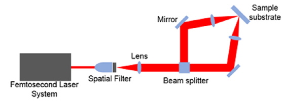
Figure 1 shows the simplified setup of the optical experiment. The fabricated Al2O3 layer was illuminated using two-beam interference to create the holographic diffraction grating pattern. The femtosecond laser system (Coherent, Chameleon Ultra II) had a center wavelength of 800 nm, a pulse width of 140 fs, and a repetition rate of 80 MHz The average power of the laser source was 3.8 W. Each femtosecond laser pulse was expanded using an objective lens embedded in a spatial filter and collimated using a lens with a focal length of 10 cm. The collimating beam was separated into two beams of identical intensity and polarization, which were directed onto the surface of the sample. Two identical lenses were used to redirect and tightly focus the beam. During the experiment the angle
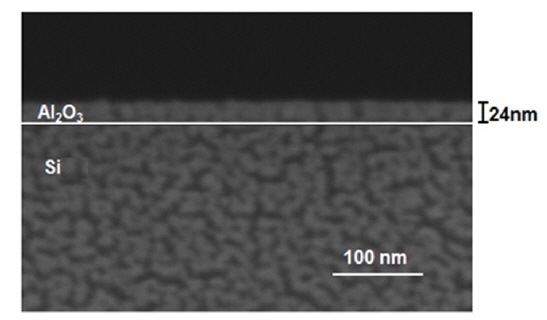
Figure 2 is a cross-section SEM image of the sample, indicating the ALD-mediated precise thickness control. Microgratings were successfully fabricated on the Al2O3 surface using the holographic grating method.
3.1. Lossless Dielectric Gratings
In accordance with Kogelnik’s method [16] for lossless or lossy dielectric gratings, the associated formula for the diffraction efficiency of a lossless grating is
Here,


In the equations above,

Here σ is the conductivity of the material, and
Using Eq. (1), the peak lossless dielectric grating efficiency was calculated as approximately 50%, occurring at
3.2. Diffraction Efficiency of Al2O3
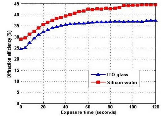
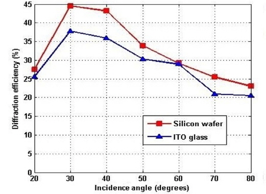
Figure 4 shows the diffraction efficiency with incident angle, in which the diffraction was measured as the ratio of the first-order diffracted light intensity to the zeroth-order diffracted light intensity. A power detector (Newport, 1835-C) measured the power and intensity of the transmitted and diffracted beams. Figure 3 shows measured data for the diffraction efficiency at a 30° incidence angle of maximum efficiency, while data for each incidence angle are given in Fig. 4. In Fig. 3 we see that the diffraction efficiencies of Al2O3 gratings on silicon wafer and ITO glass are ~45% and ~37% respectively.
According to Eq. (1), the maximum efficiency for a dielectric gratings is 50%, occurring at
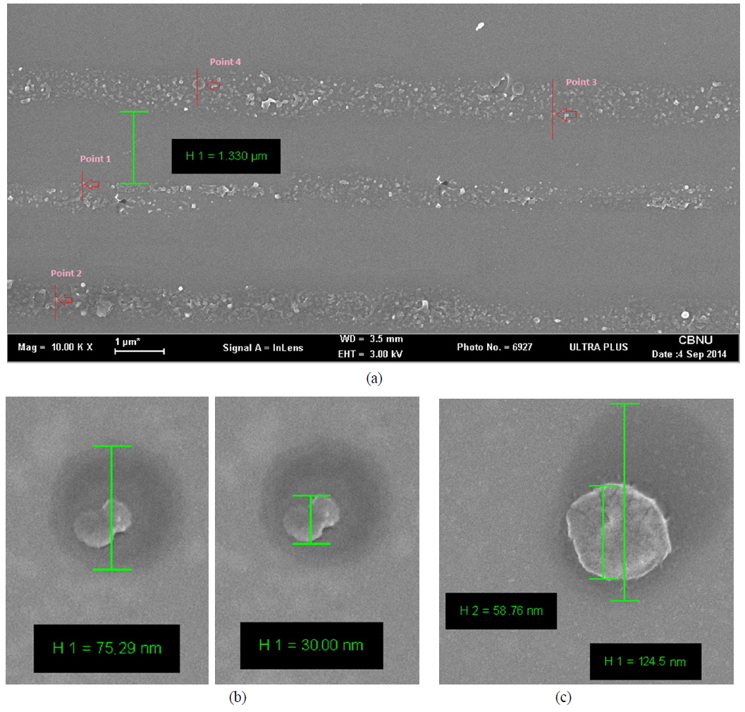
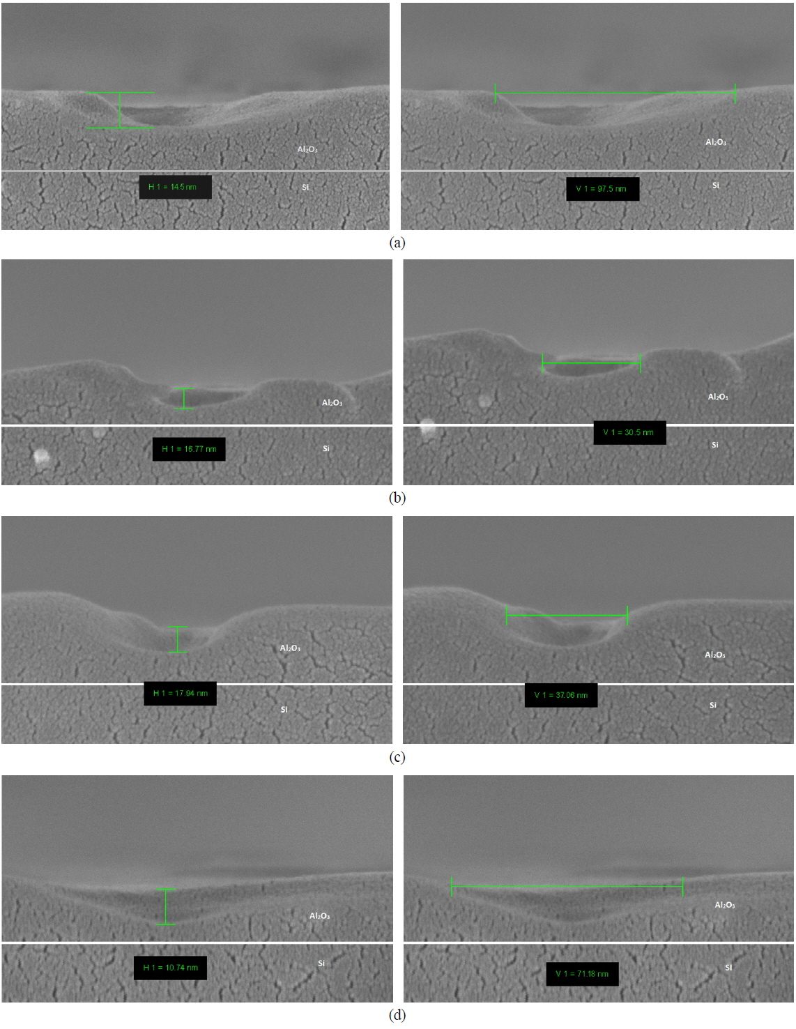
Figure 5 presents the surface of Al2O3 after irradiation for 6 hours, as seen by scanning electron microscopy (SEM). Fig. 5 (a) shows the surface with different gratings lines written by the femtosecond laser; the distance between two lines is measured as 1.330 μm. Figs. 5. (b) and (c) present burning points on the gratings, with different sizes and positions. “Point 1” (Fig. 5 (b)) has inner rim diameter of 30.00 nm and outer rim diameter of 75.29 nm, while “Point 4” (Fig. 5 (c)) has inner rim diameter of 58.76 nm and outer rim diameter of 124.5 nm.
Figure 6 shows the cross sections of some burning points on the material surface, confirming the variation of the depth of burning to range from 10 nm to 25 nm. Figs. 6 (a), (b), (c), and (d) are the cross sections of “Point 1”, “Point 2”, “Point 3”, and “Point 4” respectively. The depth and width at each of these positions are 4.5 nm and 97.5nm, 16.77 nm and 30.5 nm, 17.97 nm and 37.06 nm, and 10.74 nm and 71.18 nm respectively.
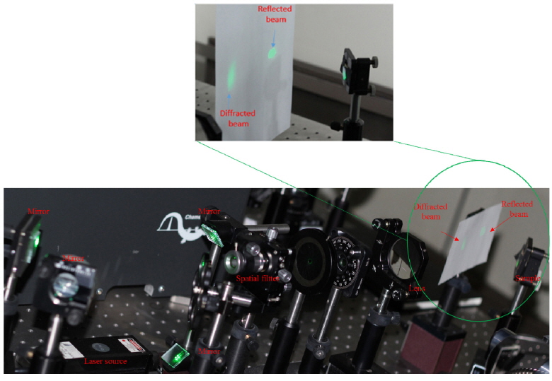
Finally, Fig. 7 shows the experiment for checking the quality of the gratings sample. In this experiment a laser beam of wavelength 532 nm, a spatial filter, and a collimating lens are used to create a plane wave. The diffracted and reflected beams are also taken on the plane. The angle between incident and diffracted beams is 30°, while the angle between the incident and reflected beams is 45°.
Relief gratings can be written on the surface of Al2O3 by the two-beam interference of individual 140-fs pulses at a center wavelength of 800 nm. The Al2O3 was deposited on a silicon substrate and on ITO glass using an ALD method, and the fabricated samples were smooth and uniform, indicating that ALD is a powerful technique for thin-film deposition, exhibiting exceptional film uniformity and precise thickness control. The diffraction efficiency was measured as approximately 45%.