검색 전체 메뉴
PDF
맨 위로
OA 학술지
Simulation Study on the Effect of the Emitter Orientation and Photonic Crystals on the Outcoupling Efficiency of Organic Light-Emitting Diodes
  • 비영리 CC BY-NC
  • 비영리 CC BY-NC
ABSTRACT
Simulation Study on the Effect of the Emitter Orientation and Photonic Crystals on the Outcoupling Efficiency of Organic Light-Emitting Diodes
KEYWORD
OLED , Outcoupling , Photonic crystal , Optical simulation
  • I. INTRODUCTION

    Organic light-emitting diodes (OLEDs) are widely used as display devices and recently began to enter the market of general lighting [1, 2]. Since the light is emitted from the organic emitting layer having a high refractive index, a substantial portion of the generated light cannot escape from the organic layers and the glass substrate due to total internal reflection (TIR) [3]. The trapped light in OLED can be categorized into the glass mode and the organic (or waveguide) mode depending on the location where it is guided by TIR. In addition, coupling of the light with the metal cathode and the resulting plasmon excitation or absorption is another loss mechanism, in particular, at a short cathodeemitter distance [4]. Therefore, enhancing light extraction efficiency has been one of the most important strategies for increasing wall-plug efficiency of OLEDs.

    There have been many theoretical and experimental efforts to improve the outcoupling efficiency (OCE) of OLEDs. For example, the glass mode can be extracted from the substrate by forming either a microlens array or a diffusing layer on the glass substrate [5-12]. The internal bulk or interface structures were modified to extract the light trapped in the organic layers by, for example, reflector modification, insertion of low-index grids in the organic layers, interface or structure modification of the organic and ITO layers, and patterning the ITO electrodes along with an insertion of a high-conductivity polymer layer [13-20]. Hybrid structures may be used to extract both the trapped light in the waveguide mode and the glass mode [21, 22]. In addition, transparent electrodes can be used to realize metal-free OLEDs, where the surface plasmon and absorption losses can be reduced significantly [23].

    Recent studies showed that it was possible to control the emitting molecular orientation, thus the emitter orientation, with respect to the normal of the OLED layers to some degree [24-29]. The emission process in OLEDs can be regarded as a dipole transition of the emissive molecules. Achieving horizontal orientation of emitting dipoles is a very favorable condition for obtaining higher OCE than vertical or isotropic orientations. The efficiency values of these oriented OLEDs were found to be much larger compared to those of conventional OLEDs. The purpose of this simulation study is to investigate the effect of the emitter orientation in the emitting layer on the OCE of bottom-emission OLED with various thicknesses of ETL. In particular, the combined effect of the emitter orientation and photonic crystals on the OCE has been investigated in detail by using the finite difference time domain (FDTD) method [30-33] and the ray-tracing technique. The detailed dependence of the OCE of OLEDs with a photonic crystal layer on the ETL thickness may be a new aspect of this study and can serve as a new, useful data set which can be considered in the optimization of the OLED layer structure.

    II. SIMULATION

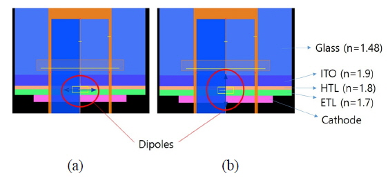
    Figure 1 shows a schematic structure of the OLED studied by the FDTD method. Commercially-available software (FDTD Solutions, Lumerical Solutions, Vancouver, Canada) was used to carry out the electromagnetic wave simulation. The OLED in Fig. 1 is bottom-emitting type consisting of a metal cathode (aluminum), an electron-transporting layer (ETL), a hole-transporting layer (HTL), an indium tin oxide (ITO) layer and a glass substrate. The simulation area was 10×10 µm2. The refractive indices of these layers (n) are shown in the same figure. The thickness of the cathode, HTL, and ITO were fixed to 100, 50, and 150 nm, respectively. A point-dipole radiation source at a wavelength of 550 nm was placed at the center of the interface between the HTL and ETL. The oscillating direction of the dipole was set to be either horizontal (a) or vertical (b) with respect to the interface.

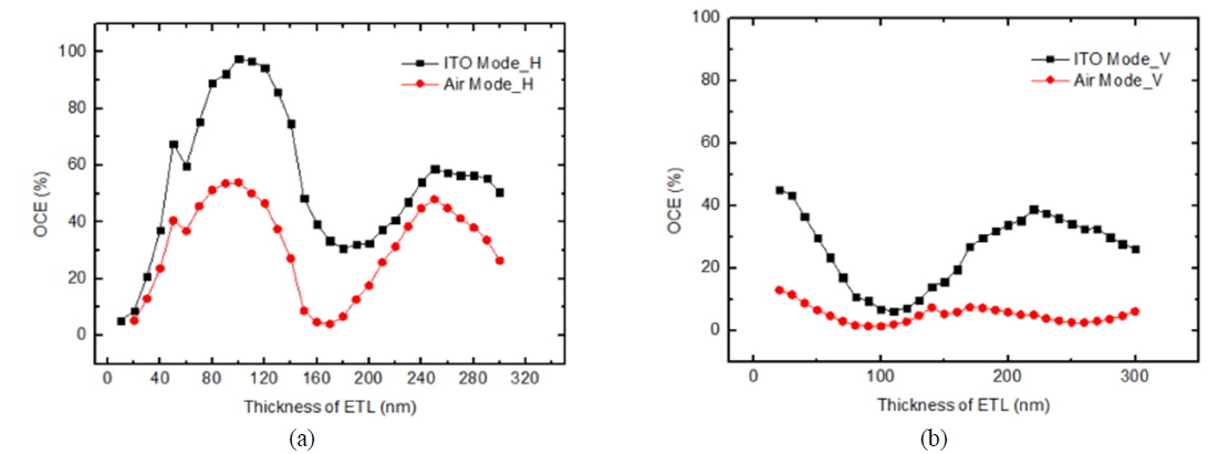
    The far-field angular radiant intensity distribution, detected in the glass substrate over the ITO layer at a distance of 95 nm, was imported into the ray-tracing software program (ASAP, Breault Research Organization, Tucson, USA), which was treated as the emitting ray distribution of an imaginary flat light source. This imaginary light source, with an area of 0.5×0.5 mm2, was located at the center of the glass substrate. The area and the thickness of the glass substrate is 2×2 mm2 and 0.7 mm, respectively. According to this procedure, we could obtain the OCE escaped from organic/ITO layers into the glass substrate (denoted as “ITO Mode”) and that escaped from the substrate into the air (denoted as “Air Mode”).

    In addition to the investigation of the basic OLED structure, a photonic crystal layer was formed on the ITO layer. The SiN cylinder (n=1.9) was put on a square lattice with a period of 500 nm. This period was found to be the optimum value for the wavelength of 550 nm [33]. Between the SiN cylinders was the glass material (n=1.48).

    III. RESULTS AND DISCUSSION

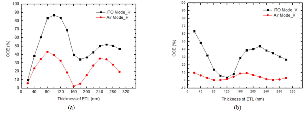
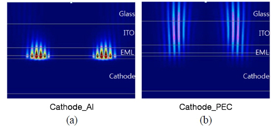
    It is well known that the interference effect between the emitter radiation with its reflected field from the cathode is critically dependent on the distance between the emitter and the cathode [2]. This two-beam interference makes the OCE oscillate with the thickness of ETL [30, 32, 33]. In addition, the surface plasmon excitation and absorption in the metal cathode is another pathway of the generated light in OLEDs into heat dissipation, in particular when the emitter is close to the cathode. The plasmon excitation loss can easily be checked if we replace the aluminum cathode by an ideal perfect electrical conductor (PEC), the reflectance of the latter being 100% without any loss. Figure 2 shows the comparison of the light intensity (proportional to the squared electric field) propagated from the vertically oscillating electric dipole. It is clearly seen that the propagation of the electromagnetic waves is localized along the cathode-ETL interface for the aluminum cathode indicating substantial excitation of the surface plasmon, while some portion of the electromagnetic waves penetrates into the ITO and the glass substrate when the ideal reflector is used as a cathode. The radiation profiles reported in Ref. 17 also revealed that the radiation emission from vertical emitters was mainly limited to large angles below the critical angle resulting in a low extraction efficiency [17].

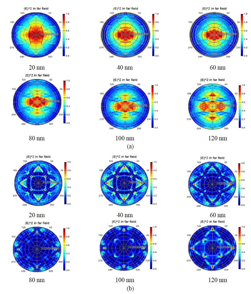
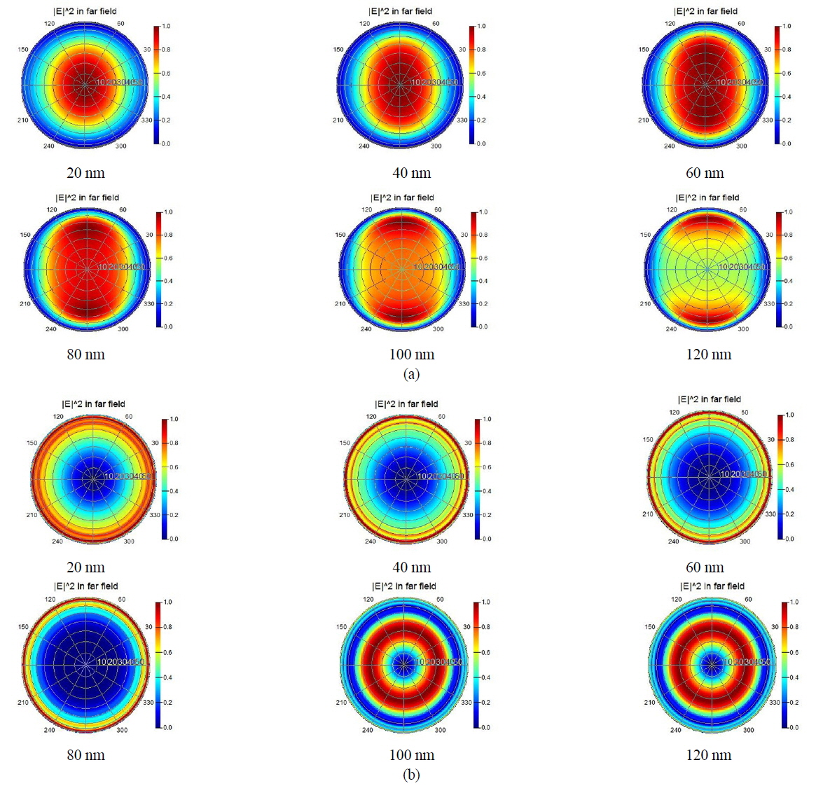
    Figure 3(a) and (b) show the polar plots of the far-field intensity distributions proportional to |E|2, where E is the electric field, detected in the glass substrate as a function of ETL thickness for both horizontal and vertical emitters. Figure 3(a) shows that the intensity along the normal direction increases and then decreases with increasing ETL thickness. On the other hand, the far-field intensity distribution of the vertical emitter shows the opposite effect, i.e., the intensity along the normal direction decreases with the increase in the ETL thickness from 20 to 120 nm. Figures 4(a) and (b) show the dependence of OCE escaped from organic/ITO layers into the glass substrate (ITO Mode) and that escaped from the substrate into the air (Air Mode) on ETL thickness for the horizontal and the vertical emitter, respectively. It becomes clear from the comparison between Fig. 4(a) and (b) that the two orthogonal emitters exhibit opposite interference conditions. For example, the first maximum of OCE (Air Mode) is located at ~ 80 nm for the horizontal emitter, which is close to the minimum of OCE for the case of the vertical emitter. This different interference effect can be explained by considering the phase relationship between the forward (towards the substrate) and backward (towards the cathode) electric fields in addition to the phase shift at the cathode. In the case of vertical emitter, the forward and the backward electric fields are initially out of phase with a phase difference of π, while they are in phase for the horizontal emitters [25]. These results clearly demonstrate that the emitter orientation is the most important factor for the OCE at a fixed emitter-cathode distance. The OCE in the “ITO Mode” and the “Air Mode” for the case of the horizontal emitter orientation are 87% and 43%, respectively, which are much larger than those for the case of the vertical emitter orientation.

    Figures 5(a) and (b) show the polar plots of the far-field intensity distributions detected in the glass substrate as a function of the ETL thickness for both horizontal and vertical emitters when the photonic crystal layer was inserted between the ITO layer and the glass substrate. (The dimensions of the SiN cylinders were optimized values as described below.) The overall change in the intensity as a function of ETL thickness is similar to the results shown in Fig. 3. However, the intensity distribution exhibits a unique pattern having a four-fold symmetry, which corresponds to the symmetry of the photonic crystal placed on a square lattice. This directional property was also observed from the intensity distribution in the “Air Mode”. The selective enhancement of the light along particular directions is one of the disadvantages of the photonic crystal structure applied to OLEDs. Addition of scattering particles in the glass substrate may reduce this directional enhancement to some degree, making the intensity distribution closer to the Lambertian distribution and thus more suitable for illumination applications [34].

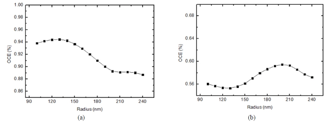
    The OCE of OLED was investigated as functions of the radius and of the height of the SiN cylinders in the photonic crystal. (The period was fixed to 500 nm according to previous study [33].) The height of the cylinder did not have substantial effect on OCE, while the radius has some effect on it. Figures 6(a) and (b) show the dependence of OCE in the “ITO Mode” on the radius of the SiN cylinder for the horizontal and the vertical emitters. According to this simulation result, optimized dimensions of the SiN cylinders could be obtained for both emitter orientations. The radius and the height of the cylinder were fixed to 130 nm and 100 nm for the horizontal orientation and 200 nm and 120 nm for the vertical orientation. Figures 7(a) and (b) display the dependence of OCE on ETL thickness for the horizontal and vertical emitters, respectively, obtained from the simulation for OLEDs having the optimized photonic crystal layer. The oscillating behavior of OCE reflects the two-beam interference effect, and the two cases exhibit almost an opposite behavior to each other. The OCE in the “Air Mode” is 54% at the ETL thickness of 100 nm in the case of horizontal orientation, while it is less than 13% over the whole ETL thickness in the case of vertical orientation. The application of the photonic crystal to the bottom-emission type OLED increases the OCE in the “Air Mode” from 43% to 54%, which indicates that the nanoscale photonic crystal layer is effective in extracting the light trapped in the organic/ITO layer. If the emitter orientation is not optimized, the OCE for the OLED with the optimized photonic crystal layer is reduced from 54% to 34.2% [33]. This study suggests that the control of the emitter orientation combined with other outcoupling structures such as the photonic crystal may be an effective way to increase the OCE of OLEDs.

    IV. CONCLUSION

    The effect of the emitter orientation and the photonic crystal layer on the OCE of bottom-emission type OLED was investigated by combined simulation of the ray-tracing technique and the FDTD method. The OLED with a horizontal emitter exhibited much larger OCE than that with a vertical emitter did, which was due to the substantial difference in the radiation pattern along with the different coupling with the surface plasmon excitation. The application of the photonic crystal between the organic/ITO layer and the glass substrate further increased the OCE by approximately 1.3 times, however, the intensity distribution was characterized by four-fold symmetry due to the square-lattice structure of the photonic crystal. The present study suggests that OCE of OLED may substantially be enhanced by controlling the emitter orientation and using other outcoupling structures such as the photonic crystal.

참고문헌
  • 1. Hong K., Lee J.-L. 2011 “Recent developments in light ex traction technologies of organic light emitting diodes,” [Electron. Mater. Lett.] Vol.7 P.77-91 google cross ref
  • 2. Brutting W., Frischeisen J., Schmidt T. D., Scholz B. J., Mayr C. 2012 “Device efficiency of organic light-emitting diodes: Progress by improved light outcoupling,” [Phys. Status Solidi A] Vol.210 P.44-65 google
  • 3. Gu G., Garbuzov D. Z., Burrows P. E., Venkatesh S., Forrest S. R. 1997 “High-external-quantum-efficiency organic light-emitting devices,” [Opt. Lett.] Vol.22 P.396-398 google cross ref
  • 4. Frischeisen J., Scholz B., Arndt B., Schmidt T., Gehlhaar R., Adachi C., Brutting W. 2011 “Strategies for enhanced light extraction from surface plasmons in organic light-emitting diodes,” [J. Photonic. Energy] Vol.1 P.011004 google cross ref
  • 5. Madigan C. F., Lu M.-H., Sturm J. C. 2000 “Improvement of output coupling efficiency of organic light-emitting diodes by backside substrate modification,” [Appl. Phys. Lett.] Vol.76 P.1650-1652 google cross ref
  • 6. Moller S., Forrest S. R. 2002 “Improved light out-coupling in organic light emitting diodes employing ordered microlens arrays,” [J. Appl. Phys.] Vol.91 P.3324-3327 google cross ref
  • 7. Chen M.-L., Wei A.-C., Shieh H.-P. 2007 “Increased organic light-emitting diode panel light efficiency by optimizing structure and improving alignment of pyramidal array light-enhancing layers,” [Jpn. J. Appl. Phys.] Vol.46 P.1521-1525 google cross ref
  • 8. Yang C.-J., Liu S.-H., Hsieh H.-H., Liu C.-C., Cho T.-Y., Wu C.-C. 2007 “Microcavity top-emitting organic light-emitting devices integrated with microlens arrays: Simultaneous enhancement of quantum efficiency, cd/A efficiency, color performances, and image resolution,” [Appl. Phys. Lett.] Vol.91 P.253508 google cross ref
  • 9. Cheng Y.-H., Wu J.-L., Cheng C.-H., Syao K.-C., Lee M.-C. M. 2007 “Enhanced light outcoupling in a thin film by texturing meshed surfaces,” [Appl. Phys. Lett.] Vol.90 P.091102 google cross ref
  • 10. Liu C.-C., Liu S.-H., Tien K.-C., Hsu M.-H., Chang H.-W., Chang C.-K., Yang C.-J., Wu C.-C. 2009 “Microcavity top-emitting organic light-emitting devices integrated with diffusers for simultaneous enhancement of efficiencies and viewing characteristics,” [Appl. Phys. Lett.] Vol.94 P.103302 google cross ref
  • 11. Nakamura N., Fukumoto N., Sinapi F., Wada N., Aoki Y., Maeda K. 2009 “Glass substrates for OLED lighting with high out-coupling efficiency,” [SID’09 Tech. Digest] P.603-606 google
  • 12. Jeong S. S., Ko J.-H. 2012 “Simulation study on the optical structures for improving outcoupling efficiency of organic light emitting diodes,” [J. Inf. Disp.] Vol.13 P.139-143 google cross ref
  • 13. Okutani S., Kamiura N., Sano H., Sawatani T., Fujita D., Takehara T., Sunohara K., Kobayashi M. 2007 “A 20.8-inch WXGA full color AMOLED display by integrating scattering reflector with micro-bumps,” [SID’07 Tech. Digest] P.173-176 google
  • 14. Sun Y., Forrest S. R. 2008 “Enhanced light out-coupling of organic light-emitting devices using embedded low-index grids,” [Nature Photonics] Vol.2 P.483-487 google cross ref
  • 15. Koh T.-W., Choi J.-M., Lee S., Yoo S. 2010 “Optical outcoupling enhancement in organic light-emitting diodes: Highly conductive polymer as a low-index layer on micro-structured ITO electrodes,” [Adv. Mater.] Vol.22 P.1849-1853 google cross ref
  • 16. Koo W. H., Jeong S. M., Araoka F., Ishikawa K., Nishimura S., Toyooka T., Takezoe H. 2010 “Light extraction from organic light-emitting diodes enhanced by spontaneously formed buckles,” [Nature Photonics] Vol.4 P.222-226 google cross ref
  • 17. Lee Y.-J., Kim S.-H., Huh J., Kim G.-H., Lee Y.-H., Cho S.-H., Kim Y.-C., Do Y. R. 2003 “A high-extraction-efficiency nanopatterned organic light-emitting diode,” [Appl. Phys. Lett.] Vol.82 P.3779-3781 google cross ref
  • 18. Tsutsui T., Yahiro M., Yokogawa H., Kawano K., Yokoyama M. 2001 “Doubling coupling-out efficiency in organic light-emitting devices using a thin silica aerogel layer,” [Adv. Mater.] Vol.13 P.1149-1152 google cross ref
  • 19. Peng H. J., Ho Y. L., Yu X. J., Kwok H. S. 2004 “Enhanced coupling of light from organic light emitting diodes using nanoporous films,” [J. Appl. Phys.] Vol.96 P.1649-1654 google cross ref
  • 20. Hong K., Yu H. K., Lee I., Kim K., Kim S., Lee J.-L. 2010 “Enhanced light out-coupling of organic light-emitting diodes: Spontaneously formed nanofacet-structured MgO as a refractive index modulation layer,” [Adv. Mater.] Vol.22 P.4890-4894 google cross ref
  • 21. Jang J.-H., Kim K.-J., Kim J.-H., Oh M.-C. 2007 “Outcoupling enhancement of OLED using microlens array and diffractive grating,” [Korean J. Opt. Photon. (Hankook Kwanghak Hoeji)] Vol.18 P.441-446 google cross ref
  • 22. Reineke S., Lindner F., Schwartz G., Seidler N., Walzer K., Lussem B., Leo K. 2009 “White organic light-emitting diodes with fluorescent tube efficiency,” [Nature (London)] Vol.459 P.234-239 google cross ref
  • 23. Kim J.-B., Lee J.-H., Moon C.-K., Kim S.-Y., Kim J.-H. 2013 “Highly enhanced light extraction from surface plasmonic loss minimized organic light-emitting diodes,” [Adv. Mater.] Vol.25 P.3571-3577 google cross ref
  • 24. Kim J.-S., Ho P. K. H., Greenham N. C., Friend R. H. 2000 “Electroluminescence emission pattern of organic light-emitting diodes: Implications for device efficiency calculations,” [J. Appl. Phys.] Vol.88 P.1073-1081 google cross ref
  • 25. Flammich M., Gather M. C., Danz N., Michaelis D., Brauer A. H., Meerholz K., Tunnermann A. 2010 “Orientation of emissive dipoles in OLEDs: Quantitative in situ analysis,” [Org. Electron.] Vol.11 P.1039-1046 google cross ref
  • 26. Flammich M., Frischeisen J., Setz D. S., Michaelis D., Krummacher B. C., Schmidt T. D., Brutting W., Danz N. 2011 “Oriented phosphorescent emitters boost OLED efficiency,” [Org. Electron.] Vol.12 P.1663-1668 google cross ref
  • 27. Liehm P., Murawski C., Furno M., Lussem B., Leo K., Gather M. C. 2012 “Comparing the emissive dipole orientation of two similar phosphorescent green emitter molecules in highly efficient organic light-emitting diodes,” [Appl. Phys. Lett.] Vol.101 P.253304 google cross ref
  • 28. Kim S.-Y., Jeong W.-I., Mayr C., Park Y.-S., Kim K.-H., Lee J.-H., Moon C.-K., Brutting W., Kim J.-J. 2013 “Organic light-emitting diodes with 30% external quantum efficiency based on a horizontally oriented emitter,” [Adv. Funct. Mater.] Vol.23 P.3896-3900 google cross ref
  • 29. Kim K.-H., Moon C.-K., Lee J.-H., Kim S.-Y., Kim J.-J. 2014 “Highly efficient organic light-emitting diodes with phosphorescent emitters having high quantum yield and horizontal orientation of transition dipole moments,” [Adv. Mater.] google cross ref
  • 30. Chutinan A., Ishihara K., Asano T., Fujita M., Noda S. 2005 “Theoretical analysis on light-extraction efficiency of organic light-emitting diodes using FDTD and mode-expansion methods,” [Org. Electron.] Vol.6 P.3-9 google cross ref
  • 31. Lee Y.-J., Kim S.-H., Kim G.-H., Lee Y.-H. 2013 “Far-field radiation of photonic crystal organic light-emitting diode,” [Opt. Express] Vol.13 P.5864-5870 google
  • 32. Jeong S. S., Ko J.-K. 2013 “Optical simulation study on the effect of diffusing substrate and pillow lenses on the outcoupling efficiency of organic light emitting diodes,” [J. Opt. Soc. Korea] Vol.17 P.269-274 google cross ref
  • 33. Jeong S. S., Choi H.-W., Ko J.-H. 2013 “Simulation study on the outcoupling efficiency and intensity distribution of photonic crystal-based organic light-emitting diodes,” [New Physics: Sae Mulli] Vol.63 P.892-899 google cross ref
  • 34. Jeong S. S., Ko J.-K. 2013 “Far-field luminous intensity distribution depending on the outcoupling structure of organic light-emitting diodes,” [J. Inf. Disp.] Vol.14 P.67-72 google cross ref
OAK XML 통계
이미지 / 테이블
  • [ FIG. 1. ]  A cross-section of the OLED studied by the FDTD method. The oscillating direction of the dipole (light source) is shown horizontally (a) and vertically (b) as arrows.
    A cross-section of the OLED studied by the FDTD method. The oscillating direction of the dipole (light source) is shown horizontally (a) and vertically (b) as arrows.
  • [ FIG. 2. ]  The propagation pattern of the squared electric field generated by the vertically-oriented oscillating electric dipole for the aluminum cathode (a) and the ideal perfect electrical conductor (b). EML (Emission layer) indicates the interface between the ETL and the HTL layer.
    The propagation pattern of the squared electric field generated by the vertically-oriented oscillating electric dipole for the aluminum cathode (a) and the ideal perfect electrical conductor (b). EML (Emission layer) indicates the interface between the ETL and the HTL layer.
  • [ FIG. 3. ]  Far-field intensity distribution proportional to |E|2, where E is the electric field, detected in the glass substrate as a function of the ETL thickness for (a) horizontal and (b) vertical emitters.
    Far-field intensity distribution proportional to |E|2, where E is the electric field, detected in the glass substrate as a function of the ETL thickness for (a) horizontal and (b) vertical emitters.
  • [ FIG. 4. ]  The dependence of OCE escaped from organic/ITO layers into the glass substrate (ITO Mode) and that escaped from the substrate into the air (Air Mode) on the ETL thickness for (a) the horizontal and (b) the vertical emitters.
    The dependence of OCE escaped from organic/ITO layers into the glass substrate (ITO Mode) and that escaped from the substrate into the air (Air Mode) on the ETL thickness for (a) the horizontal and (b) the vertical emitters.
  • [ FIG. 5. ]  Far-field intensity distribution proportional to |E|2, where E is the electric field, detected in the glass substrate as a function of the ETL thickness for (a) horizontal and (b) vertical emitters for the OLED with the photonic crystal layer on the ITO layer.
    Far-field intensity distribution proportional to |E|2, where E is the electric field, detected in the glass substrate as a function of the ETL thickness for (a) horizontal and (b) vertical emitters for the OLED with the photonic crystal layer on the ITO layer.
  • [ FIG. 6. ]  The dependence of OCE in the “ITO Mode” on the radius of the SiN cylinder for (a) the horizontal and (b) the vertical emitters.
    The dependence of OCE in the “ITO Mode” on the radius of the SiN cylinder for (a) the horizontal and (b) the vertical emitters.
  • [ FIG. 7. ]  The dependence of OCE on ETL thickness for (a) the horizontal and (b) vertical emitters.
    The dependence of OCE on ETL thickness for (a) the horizontal and (b) vertical emitters.
(우)06579 서울시 서초구 반포대로 201(반포동)
Tel. 02-537-6389 | Fax. 02-590-0571 | 문의 : oak2014@korea.kr
Copyright(c) National Library of Korea. All rights reserved.