In this paper, the scheme of a single module for simultaneous operation of all-optical computing circuits, namely half adder and half subtractor, are realized using semiconductor optical amplifier (SOA) based logic gates. Optical XOR gate by employing a SOA based Mach-Zehnder interferometer (MZI) configuration is used to get the sum and difference outputs. A carry signal is generated using a SOA-four wave mixing (FWM) based AND gate, whereas, the borrow is generated by employing the SOA-cross gain modulation (XGM) effect. The obtained results confirm the feasibility of our configuration by proving the good level of quality factor i.e. ~5.5, 9.95 and 12.51 for sum/difference, carry and borrow, respectively at 0 dBm of input power.
The increasing demand for high speed forced the modern research trends to ultra-fast all-optical signal processing. All-optical signal processing enhances speed and capacity of the core optical networks by avoiding expensive, time consuming and power hungry optoelectronic conversions. Among them one can cite optical clock recovery, wavelength conversion, all-optical bit logic operations, all-optical arithmetic operations and many more. Nowadays, all-optical arithmetic based devices are of great interest for research. In particular, all-optical half adder and half subtractor obtained from SOA-based all-optical logic gates have great importance as basic building modules in the development of an all-optical super-fast arithmetic logic unit (ALU) [1]. Half adder and half subtractor provide superfast ALU operation ability for implementing the different types of computation necessary to enhance the speed.
Several methods of designing all-optical half adder & half subtractor have already been demonstrated by various researchers using nonlinear optics [2-4]. Of the many nonlinear technologies investigated, semiconductor-based technologies are the most promising. SOA have been extensively investigated as basic building blocks because of their highly nonlinear characteristics and potential advantages of integration, compactness, reliability and cost effectiveness [5-7]. By using SOA as nonlinear medium, various all optical logic gates and complex circuits were proposed and also successfully implemented [8-10]. Gayen
Unfortunately, these techniques are based on costly components and limited as to the bit rate. In this paper, we have proposed a scheme which offers a single module for simultaneous operation of half adder and half subtractor at high bit rates using a SOA. After the introductory part, Section II describes the basic principles used for design of SOA based gates. The system setup and SOA’s parameters used in the setup are discussed in Section III. Section IV represents results and discussions. Finally, conclusions are drawn in Section V.
Half adder and half subtractor are combinational circuits capable of adding and subtracting two single bit numbers respectively and of producing outputs as sum and carry for an addition operation, difference and borrow for subtraction [3, 4]. The truth table of the half adder and half subtractor is shown in Table 1 with required logic gate operation necessary to implement its function.
[TABLE 1.] Truth Table of Half-Adder and Half Subtractor
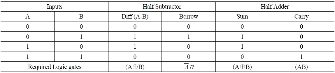
Truth Table of Half-Adder and Half Subtractor
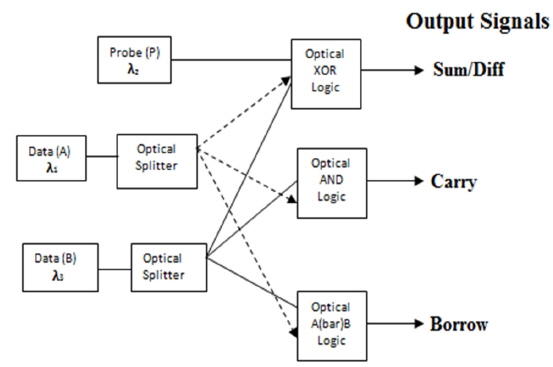
As shown in Table 1, the sum and difference can be modeled by XOR logic. On the other hand, carry and borrow logic can be modeled by AND and logic, respectively. Thus, three logic functions in the optical domain are required to implement an all-optical half adder and half subtractor. The proposed design uses a SOA-MZI configuration to implement the optical XOR logic where XPM helps to achieve the switching action. Optical AND logic is implemented using SOA-FWM, whereas is designed using XGM in SOA.
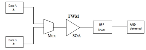
Optical AND logic is implemented using FWM in the SOA. When both the data streams, data A & data B, are simultaneously present in the SOA, then FWM of these data signals will take place [20]. It must be noted that FWM depends upon various parameters such as wavelength separation between input signals, input power levels and SOA’s parameters. So these parameters must be taken so that FWM in the SOA enhances to achieve AND operation. Due to FWM interaction, new signals at different wavelengths are generated, but with lower power levels [21]. The new generated wavelength with more power is filter out to get AND operation. Due to lower efficiency of FWM, optical filter at high bandwidth is required for desired AND gate operation. The SOA-FWM based AND design is shown in Fig. 1.
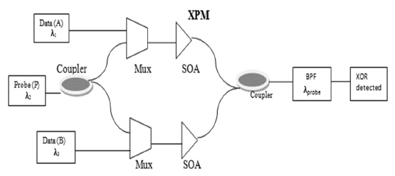
Optical XOR logic is obtained by using two SOAs in MZI configuration as shown in Fig. 2. The SOA-MZI configuration is most promising because of its simplicity, stability and versatility to different modulated input signal formats [17-19]. Two optical signals, data A and probe, are shot together in the upper arm of the SOA-MZI whereas data B and probe are injected in the lower arm of the SOA-MZI. The variation on the carrier density not only affects the optical gain but also induces a change on the refractive index [20], as a result, the phase of the probe signal gets modulated and optical XOR logic is achieved at probe wavelength.
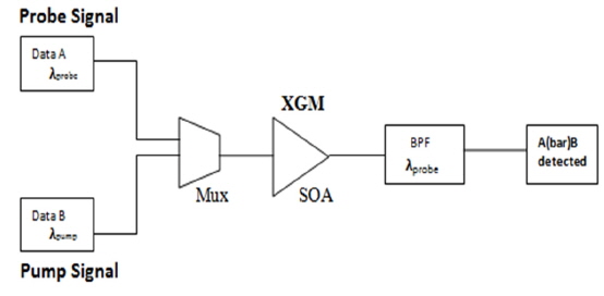
The optical logic used to get the borrow output of the optical half subtractor is implemented by employing XGM in SOA. XGM is a result of gain saturation in SOA [20]. It occurs, when a high power pump signal and a low power probe signal are simultaneously injected into a SOA as shown in Fig. 3. The pump signal causes the carrier depletion by changing the available carrier density for amplification and thus decreases the available gain to the probe signal i.e. when data bits of pump signal are high, it saturates the SOA as a result the bits on the probe signal get suppressed. Thus, to achieve optical logic, data A acts as probe signal and data B acts as a pump signal. Similarly, can also be realized simply by inversing the position of data signals. The Fig. 3 shows the design using SOA-XGM. The optical signal is detected by using an optical filter tuned at the probe signal wavelength.
The block diagram of the simulation setup to realize the half adder and half subtractor is shown in Fig. 4. The two data streams, data A at wavelength 1550 nm and data B at wavelength 1555 nm are generated using the continuous wave (CW) laser sources. The lasers are modulated according to the data provided by the user in a user-defined bit sequence generator at 40 Gbps (average) of speed. Another CW laser source is used to generate a probe signal at 1540 nm of wavelength. Both data streams are split into three branches, one branch of each data stream is fed into the SOA-MZI based optical XOR logic gate, the second branch is fed into the SOA-FWM based optical AND logic gate and the third branch is inserted into the SOA-XGM based optical logic operation. The optical power levels for input data signals are adjusted in such a way that they are compatible with all the three optical logic functions used to drive the system outputs. Optical attenuators and an optical amplifier are used to get the desired power levels necessary to operate the logic gates. The various SOA parameters that need to be adjusted for optimum SOA performance are listed in Table 2.
[TABLE 2.] The list of SOAs parameters used in the simulation

The list of SOAs parameters used in the simulation
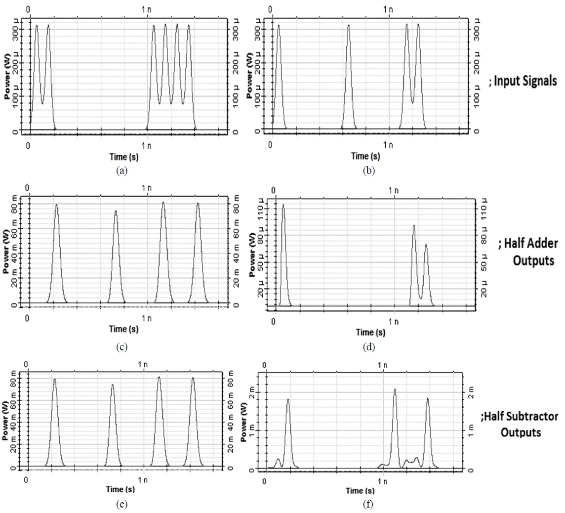
Optical half adder and half subtractor results are verified in accordance with the truth table listed in Table 1. The design performance is checked, by checking its response to different input bit sequences. The results show its compatibility with any input bit sequence. For demonstration the input data A as 1100000000111100 and data B as 1000001000011000 are considered along with output signalssum, carry, difference and borrow, as shown in Fig. 5.
The optical pulses govern amplification when propagating inside the SOA; the amplifier gain is different for different parts of the pulse. The leading edge experiences full gain as the amplifier is not yet saturated whereas the trailing edge experiences least gain since the whole pulse has saturated the amplifier gain [22].
Figure 5 also represents the power levels of all data bits transmitted through the SOAs and received as sum, difference, carry and borrow at the receiver side. It can be observed that, the proposed circuit provides better performance in the extinction ratio. But in the case of borrow (as shown in Fig. 5(f)) the extinction ratio is degraded due to the change in power seen at bit “0s”, because of XGM. However, the extinction ratio is the efficiency with which the transmitted optical power is modulated over the transmission system. It is simply the relationship of the power used in transmitting a logic level “1” to the power used in transmitting a logic level “0” [23].
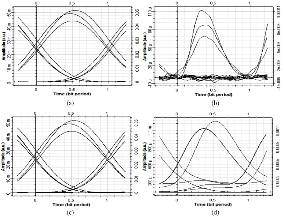
The eye diagrams of output signals are shown in Fig. 6. It can be observed that the carry operation using a SOA-FWM based optical gate limits the performance because of its dependence upon various parameters for proper occurrence and low conversion efficiency whereas the sum/difference and borrow obtained from SOA-XPM and SOA-XGM show better switching operation, and their performance is limited by carrier recovery time of the SOA only.
The quality factor performance is observed to analyze the electrical signal, which is recovered from received optical pulses. Table 3 described the Quality factor performance as a function of input power with respect to all considered operations (i.e. XPM, FWM and XGM). It can be seen that all operations have been achieved with acceptable Quality factor (i.e. > 5.7) even at all worst cases (i.e. at high input power and bit rate). Best performance has been seen at 0 dBm of input power for all logical operations.
[TABLE 3.] Quality factor performance of the system at different input power levels
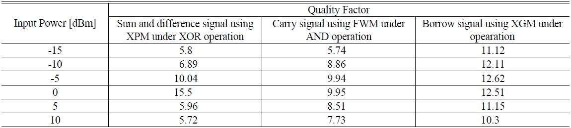
Quality factor performance of the system at different input power levels
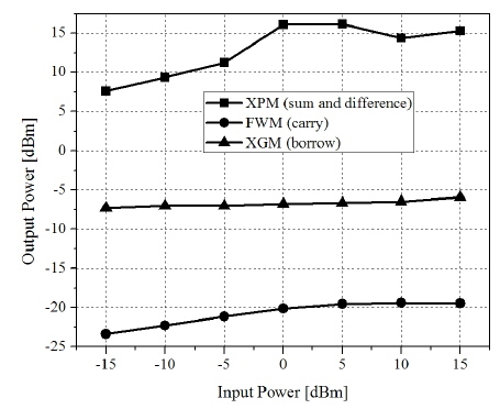
For the better clarity, we have also investigated the influence of FWM, XPM and XGM in the term of output power. Figure 7 represents the variation of output power, due to FWM, XPM and XGM, with respect to input power per channel. It can be observed that sum or carry (due to XPM) and borrow (due to XGM) provides better power level as compared to carry (due to FWM). The AND (or carry) output has a low power level due to the low conversion efficiency of the FWM.
4.1. Comparison of Proposed System with Existing Investigations
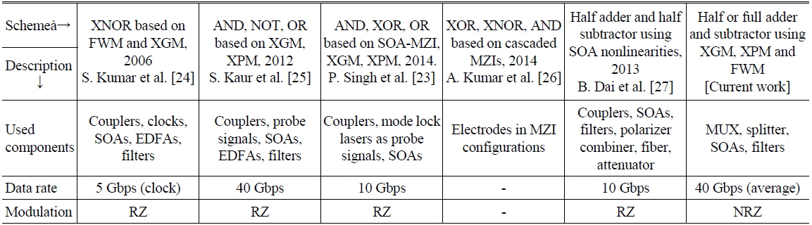
In this section, we compare the important performance parameters of our proposed system with current state-of-the-art schemes [23-27], as described in Table 4. This comparison has been done to determine the level of knowledge and the development achieved in a technique. From this table it can be concluded that our proposed system shows improvement over currently published research because: (1) we achieve better performance using simple configuration and operation by omitting the requirement of costly components, such as an erbium doped fiber amplifier (EDFA) for amplification, cascaded MZI configurations, etc. (2) The reported results have been conducted for half adder and half subtractor (i.e. combinations of more than one optical gate), even at high data rate with acceptable performance. From this survey, it can be observed that the performance of the current proposed system can be extended by proposing the new high level architecture (i.e. arithmetic and logic unit, photonic processor, memory etc.) using proposed combinational circuits and other gates.
[TABLE 4.] Comparison of our proposed system with currently published schemes reported in [23-27]
Comparison of our proposed system with currently published schemes reported in [23-27]
All-optical half adder and half subtractor are successfully demonstrated using SOA based optical logic gates. The proposed design has simplicity and compatibility with all input bit sequences. The system is analyzed in terms of input-output bit operation and eye diagrams. Due to the multifunctions and the use of integrable components, the proposed scheme has the potential to be applied for future optical systems, such as arithmetic logic units and encryption/decryption devices.


![Comparison of our proposed system with currently published schemes reported in [23-27]](http://oak.go.kr/repository/journal/16133/E1OSAB_2014_v18n6_639_t004.jpg)