Liquid crystal displays (LCDs) are a non-emissive type display that modifies the polarization of input light coming from a backlight unit by controlling electrically the retardation of liquid crystals. Many liquid crystal modes adopted in the initial stages of liquid crystal displays (LCDs) have disappeared from the display market due to customer demands for higher image quality. Only LC modes with excellent electro-optical properties, e.g., vertical alignment (VA) type nematic modes [1-3], in-plane switching (IPS) mode [4], fringe field switching (FFS) mode [5], twisted nematic mode (TN) [6], and optically-compensated bend (OCB) mode [7-9], have survived in various display applications.
Among the LCD modes, VA-type LCD modes, e.g., multi-domain vertical alignment (MVA) and patterned vertical alignment (PVA) nematic modes, have several merits, such as rubbing free process, wide viewing angle, low driving voltage, and high contrast ratio in the normal direction. Therefore, VA-type modes have been investigated by many engineers and scientists and used widely in larger sized displays, such as TVs. On the other hand, they also have demerits, such as slow rising speed and low transmittance, due to the disclination of LC molecules driven from direction matching between the electric field direction and initial LC alignment in the vicinity of the middle region of electrodes, leading to an almost vertical field [1].
To solve these issues, i.e., to eliminate the disclination and improve the rising speed, Kim
This paper proposes an improved vertical alignment nematic mode with the protrusions of the top substrate and stripe type common electrodes with polarity switching of the bottom substrate to improve the MVA and PVA nematic modes, which have demerits, such as an LC disclination in the vicinity of the middle region of the electrodes between the top and bottom protrusions in MVA mode or top and bottom slits in PVA mode. Here, the stripe type common electrode and the protrusion or the slit will play important roles in preventing LC disclination. Therefore, the proposed VA mode will have higher transmittance than the MVA and PVA modes. As a result, the proposed VA mode can improve the response speed and transmittance remarkably.
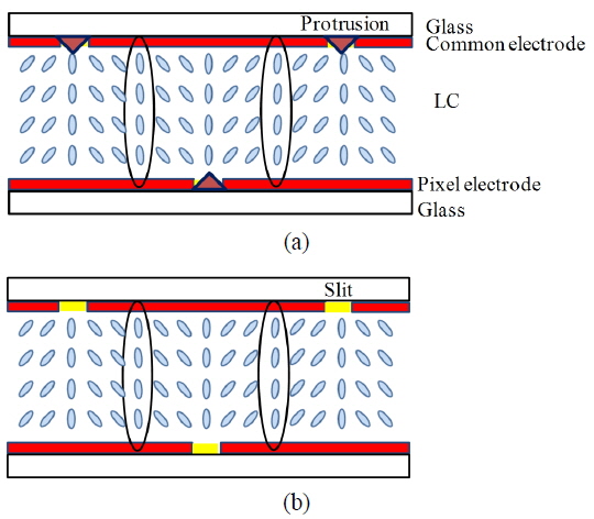
Figure 1 (a) and (b) present schematic diagrams of the LC director behaviors under an electric field by the common electrode and the pixel electrode in the cell structure of the conventional MVA and PVA modes, respectively. As indicated in Fig. 1 (a) and (b), the LC directors in the black circle region between the top protrusion (or slit) and bottom protrusion (or slit) exhibit disclination behavior because the electric field at the region is almost vertical. In a more detailed description, vertically aligned negative LCs show random azimuthally laying directions because of the vertical electric field coincident with the long axis of LC at this region. Therefore, LCs experience transient disclination formation until propagated to the LCs of the middle region (the black circle region) from the LCs in the vicinity of the protrusion (or slit). Because of this, the response speeds of the MVA and PVA modes are slow at the rising time. High transmittance can be obtained if the distance between the top and the bottom protrusions (or slits) is widened. On the other hand, the response speed is slower because the time of propagation to the LCs of middle region from LCs of the protrusion (or slit) is longer. Eventually, the distance cannot be widened and the transmittance cannot be enhanced in conventional MVA and PVA configurations.
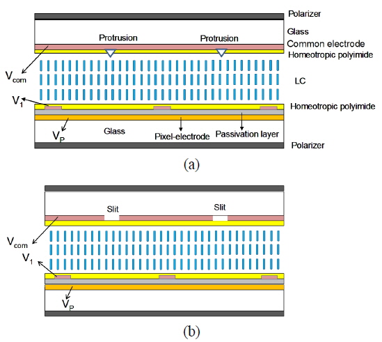
To increase the transmittance in the VA LC structure, this paper proposes a new electrode structure and its switching method. Figure 2 shows a schematic diagram of the unit LC cell in the proposed VA configuration. The purpose of this configuration is to tilt the vertical electric field slightly between the bottom pixel electrode and the top common electrode so that the LCs of the middle region can lie down instantly according to the tilted field.
In a detailed description of the proposed VA structure, wholly indium-tin-oxide (ITO) coated electrodes were positioned on both glass substrates. The entire area-ITO coated electrode on the top substrate was used as the common electrode, and the protrusions in Fig. 2 (a) and the slits in Fig. 2 (b) were produced by an etching process. The polyimide (PI) for homeotropic LC alignment was placed on the electrodes. For the bottom substrate, the entire area-ITO coated electrode on the bottom substrate was used as the pixel electrode connected with a thin film transistor (TFT). The passivation layer (insulator) was deposited on top to prevent electrical short between the pixel electrode (TFT-electrode) and the stripe type common electrode.
In the operation of this electrode structure, the potential difference between the pixel electrode (VP) and the common electrode (Vcom) induces a vertical electric field, whereas the electrical potential difference between the pixel electrode and the stripe type common electrode (V1) leads to a horizontal electric field. The electrical potential difference between the common electrode and stripe common electrode generates a tilted electric field, albeit a weak field, and the tilt differs according to the position. Consequently, mixing of the vertical electric field and the horizontal field produces a tilted electric field preventing LC disclination formation, even in the middle region between the protrusion or slit and the stripe type common electrode. This is the concept for enhancing the transmittance of the VA mode.
In a switching skill, constant voltage was applied to the common electrode. On the other hand, the electric polarity of the stripe type common electrode should be changed every frame, even though the magnitude of applied voltage is constant. In addition, an apposite polarity to the polarity of pixel electrode is always needed to maintain the same electric field direction within an LC domain.
A commercial LCD simulator from Techwiz LCD was used to examine numerically the electro-optics of the proposed VA mode. The LC material and cell thickness used for the simulation were MLC-6610 (Merck), which has Δn=0.09 (Δε=−3.1) and 3.4 μm, respectively.
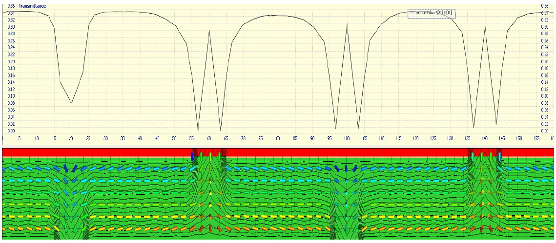
Figure 3 presents the transmittance according to the position of the pixel when 8 V is applied to the pixel electrode in conventional PVA (or MVA) mode. As shown in fig. 3, the transmittance of the PVA mode is not high because the transmittance always decreases at each slit region. In addition, the vertical electric field of the center region between the top and bottom slits confuses the vertically aligned LCs on the decision of the azimuthally lying direction, called the disclination formation of LCs. Here, the calculated angular value of the electric field was 89.2° in the middle region. Therefore, the response speed of the MVA or PVA modes is reduced. In addition, an expansion of the distance between the slits was performed to increase the transmittance. On the other hand, its expansion aggravates the disclination formation of the LCs to the wider region and the response speed is slower. Here, the distance between slits was 30 μm and the width of the slit was 10 μm.
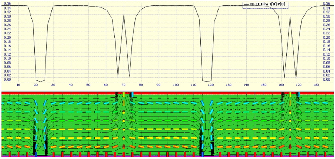
Subsequently, the proposed VA mode was simulated as an electrode structure shown in Fig. 2. In the simulation, the constant voltages to the common electrode and the stripe type common electrode were 0 V and 1.5 V (−1.5 V), respectively, to induce a horizontal electric field in the pixel. Here, 1.5 V (−1.5 V) is below the threshold voltage of MLC-6610. The voltage VP of the pixel electrode connected to the TFT was varied to 8 V from 0 V. The horizontal fields between the pixel and the stripe type common electrodes and between the common and the stripe type common electrodes prevent the formation of LC disclination due to matching of the LC direction and the vertical field between the pixel and common electrodes. Owing to this horizontal field, the proposed VA mode can expand the distance between the slits, unlike the MVA and PVA modes. Therefore, in this simulation, the distance between the slits was expanded to 40 μm.
Figure 4 shows the LC director behavior, equipotential and transmittance according to the position in the pixel under the electric field of the proposed VA mode. As expected, the equipotential lines were not flat when VP is 8 V. Here, the calculated angular value of the electric field was 87.7° in the middle region due to the horizontal field. This means that the vertical field generating no azimuthal preference direction of LCs is tilted slightly in between the slits, even though the distance between the slits is 40 μm, which is wider than that of typical MVA or PVA modes with 30 μm. As a result, the proposed VA mode can lead to a faster response speed than the PVA mode. Therefore, the distance between the slits can be increased, which will increase the transmittance.
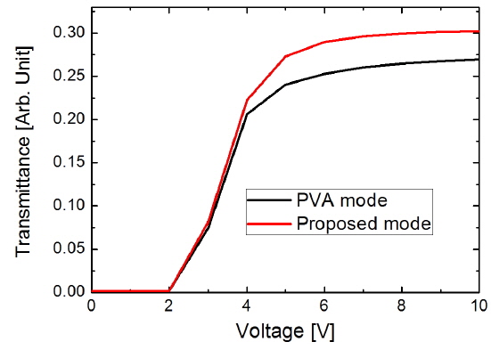
Figure 5 compares the voltage-transmittance curves of the proposed mode with the electrode structure of 5 μm (the width of the slit): 40 μm (the distance between the top slit and the bottom slit) with those of the typical PVA mode with 10 μm (the width of the slit): 30 μm (the distance between the top slit and the bottom slit). As expected, the transmittance increased slightly with increasing distance between the slits. As a result, the proposed structure showed higher transmittance than the typical PVA mode. The transmittance of VA mode was enhanced by 8.5 % compared to the PVA mode.
Finally, to determine if the response speed of the proposed VA mode is faster than that of the conventional PVA mode, the response time of the proposed VA was compared with that of the conventional PVA through a simulation, even though the absolute value of response time at the used simulator is not known. As a simulated result, the response speed of the proposed VA mode with an electrode structure of 5 μm : 40 μm was 1.3 times faster than that of the conventional PVA mode with the same electrode dimension and 1.1 times faster than that of the conventional PVA mode with an electrode structure of 10 μm : 30 μm. Consequently, the proposed VA mode in the response time remains intact despite the wider distance between the top and bottom slits to obtain higher transmittance.
This paper presented, as an improved vertical alignment nematic liquid crystal mode, a new vertically aligned nematic mode with the protrusions or the slits of the top substrate and stripe type common electrodes of the bottom substrate. The proposed VA mode had enhanced characteristics compared to the MVA and the PVA nematic modes with a LC disclination in the vicinity of the middle region of the electrodes between the top and bottom protrusions in the MVA mode or the top and bottom slits in PVA mode. The LC disclination was improved using the stripe type common electrode generating a horizontal electric field and the protrusions producing some pretilt of the liquid crystals (LCs). The simulations showed that the proposed VA mode had higher transmittance than the MVA and the PVA modes. Consequently, the proposed VA mode can improve the response speed and transmittance, and it is useful for upgrading the LCD display quality.