In recent years, boron nitride (BN) has attracted the attention of researchers. Crystalline BN exhibits several crystal structures, including hexagonal and cubic forms. Hexagonal boron nitride (h-BN) has a two-dimensional honeycomb lattice structure, similar to that of graphene. However, in contrast to graphene, h-BN is a well-known insulator with a high thermal conductivity. [1, 2] Graphene nanodevices with an h-BN substrate show better electronic properties than those with the standard SiO2 substrate. [3-5] Moreover, the h-BN substrate has an advantage, in that its surface is flatter than other substrates. [4, 5] In fact, the surface roughness is not only less than for SiO2 on a h-BN monolayer, but also it becomes about a third of that for SiO2 when the h-BN thickness is about 14 nm. [3, 4]
It is important to accurately measure the thickness of h-BN and characterize its surface, due to the need for very thin h-BN films in many studies and devices. Thin h-BN flakes with less than 100 layers can easily be obtained using the standard cleaving [6] or mechanical exfoliation methods. [7] For graphene, which has a two-dimensional structure similar to that of h-BN, methods such as Raman scattering [11], atomic force microscopy (AFM) [12], and optical contrast [8-10] have been used to identify thickness and surface properties. In the case of h-BN, the reflectivitycontrast method [13, 14] and Raman scattering [13] have been used. The reflectivity-contrast method using a specific wavelength is not only simple and convenient, but also cost effective, as opposed to other methods, which are time-consuming and expensive.
Optical methods have been used to observe the properties of the thin film [15, 16]. Here, to determine the thickness of an h-BN flake, we propose an improved method that is more accurate and effective than the standard optical reflectivity-contrast method. We use the wavelength of zero contrast plus the linear change in zero-contrast wavelength with thickness of h-BN, instead of the nonlinearly changing extremes of optical contrast. To confirm the accuracy of this approach, we compare its results to those from AFM measurements.
Multilayer h-BN flakes were prepared by mechanical exfoliation from powders (PT-110, Momentive Performance Materials) with an average particle size of about 45 μm. [7] The multilayer h-BN flakes were attached to a SiO2/Si substrate that was 276 nm thick. The thickness of the SiO2 layer was measured by spectroscopic ellipsometry. To measure the reflectivity, we used an optical microscope objective (100×, NA = 0.8, Eclipse E600 POL, Nikon) with a halogen lamp as a source of white light. The light was focused on the h-BN flake and the effectively parallel light injected vertically into the flake. The intensity spectrum of the reflected light was obtained using a spectrometer with a resolution of 0.24 nm (USB4000, Ocean Optics) attached to the microscope. The h-BN flakes were chosen to be larger than the spot size of 3 μm.
Wavelength-dependent contrast in the experiment is defined as the normalized difference between the light reflected by SiO2 and by the h-BN flake. The light reflected from the SiO2 is used as the reference, and the contrast (=(RSiO2 − Rh-BN))/RSiO2) can be calculated [14]. RSiO2 is the intensity of light reflected from the SiO2/Si substrate at a given wavelength λ, and Rh-BN is the intensity of light reflected from the h-BN flake on the substrate.
We used a multilayer interference approach to determine the number of h-BN layers from the optical contrast [17]. Assume a multilayer system with index j in {1, 2, 3} for our system. Index 1 corresponds to the h-BN flake, and indices 2 and index 3 to the SiO2 layer and Si substrate respectively. Following the standard calculation using a transfer matrix, the multilayer reflection coefficient at a layer is related to other coefficients as follows [14]:

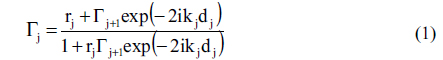
Here Γj is the ratio of the total electric field of an incident (Ej+) and a reflected (Ej−) wave at the jth interface, expressed as Γj = Ej−/Ej+. Γj is a reflection coefficient that includes the effects of other layers of higher index value. rj is the reflection coefficient at the jth interface, expressed as rj = (nj−1)/(nj−1+nj), being the refection coefficient at an interface consisting of two semi-infinite materials. kj(=2 πnj/λ) is the wave vector and dj the thickness of the jth layer. The h-BN flake and SiO2 film have refractive indices n1 and n2 and thicknesses d1 and d2 respectively, and are positioned between the air (n0 = 1) and the Si substrate (n3). [18] Both air and Si substrate are assumed to be infinitely thick. n1 shows a linear variation (n1 ≈ 2.23 − 6.9λ × 10−4) in the wavelength range 480-640 nm. [19] n2 and n3 were also frequency-dependent, but nonlinear with frequency. [20] Notthae t the value for the refractive index of Si (n3) indicates an absorption with imaginary value, which was applied in the calculation. The reflection coefficient at the interface between SiO2 and Si is set to Γ3 = r3. We can calculate the optical contrast using Rh-BN = ∣Γ1∣2 and RSiO2 = ∣Γ2∣2 as a function of the number of layers of h-BN. We fitted the calculated optical contrast to the measured values for samples with varying numbers h-BN layers, and compared the fitted results to AFM measurements. The very low thickness of the h-BN flake and modest reflectivity at the interface yield very low wavelength resolution, with negligible change in the interference across the visible range.
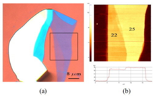
Figure 1(a) shows an optical-microscopy image of an h-BN flake on a SiO2/Si substrate. The flake has several regions with different thicknesses, and consequently different reflectivities. Figure 1(b) shows an AFM image of the same flake, to identify the regions with different thicknesses; the lower panel shows the height profiles taken along the red horizontal line in the image above. The number of h-BN layers can be calculated by dividing the flake thickness by the thickness of a single layer (0.33 nm).
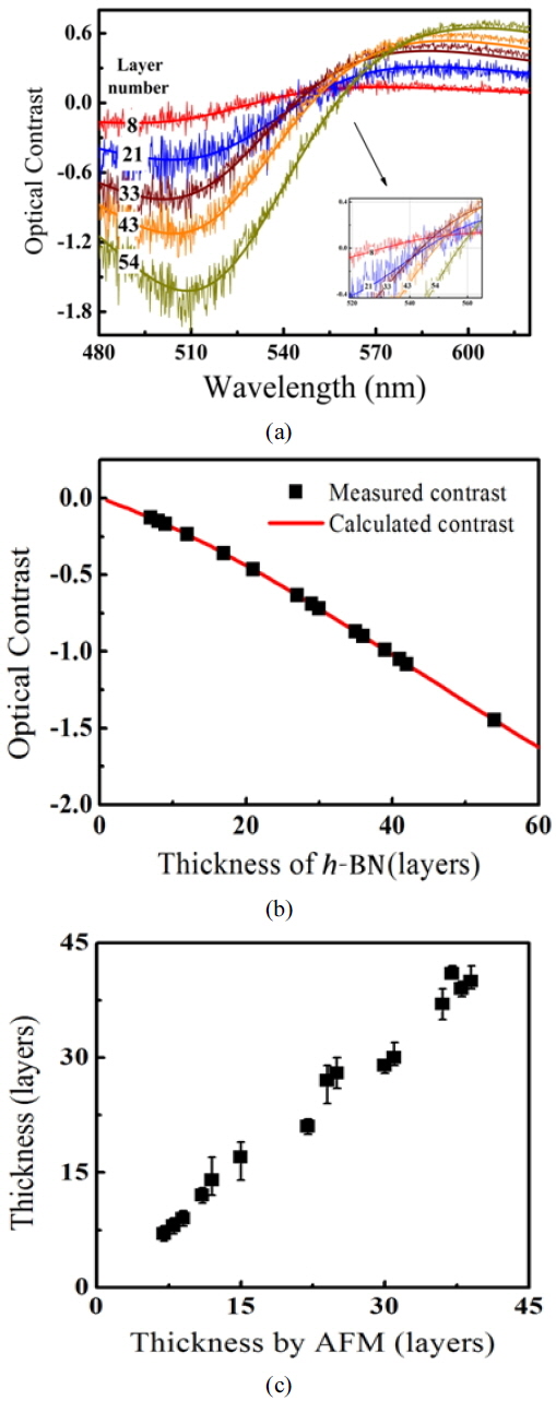
Figure 2(a) shows the optical contrast for several h-BN flakes of different thicknesses, as a function of wavelength. The number of layers was determined by numerical fitting to experimental results, as described above. Depending on the visible wavelength, the optical contrast may be negative, zero, or positive. The change of sign in the optical contrast seems to be due to variation in the refractive index of the materials; however, it is not simple to guess the zero-contrast point with the equation. The minimum and maximum values increase proportionally to the number of layers. In particular, the contrast variation per layer is greatest (2.8-2.9%) for wavelengths between 510 and 524 nm. The human eye can detect a thin layer using light in this range. [14]
We can determine the number of layers by the variation in optical contrast at a single wavelength. As can be seen in Fig. 2(b), the contrast at 513 nm (the wavelength corresponding to the largest rate of variation) changes comparatively linearly for thick h-BN flakes. The solid red line and black squares respectively represent the calculated contrast at 513 nm as a function of the number of layers and the measured optical contrast. The calculated contrast values seem to match the experimental results well. The rate of contrast variation is approximately 2.9% per layer, which means that the number of layers can be determined by analyzing the spectrum of reflected light. However, the optical contrast is considered to be susceptible to the thickness of the SiO2 layer, and to any water adsorbed on the h-BN. [13, 14] Hence the exact number of layers cannot be determined using only the contrast at a specific wavelength, because other factors lead to non-negligible error. Moreover, the contrast variation is nonlinear for the first 15 layers, as indicated by the red solid line in Fig. 2(b).
To gauge the accuracy of this method, we compare its results to the number of layers measured by AFM (Fig. 2(c)). The values obtained by fitting the optical contrast do not match the AFM measurements well enough. The error bars indicate that the optical-contrast method yielded different thicknesses than the AFM measurements. These differences may be due to the susceptibilities of the optical-contrast mentioned above.
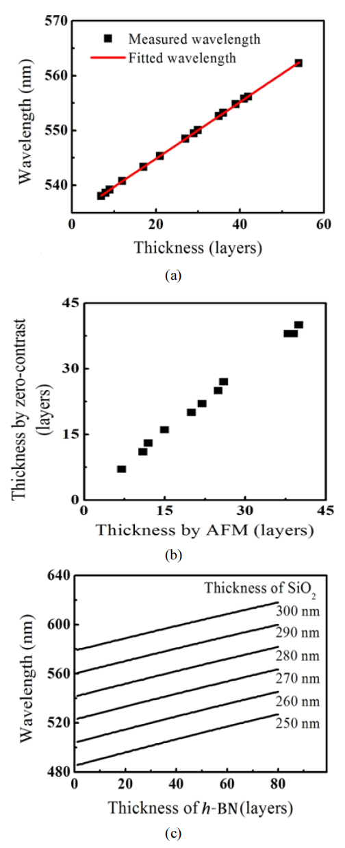
To determine the number of layers as efficiently as possible, we analyzed the change in optical contrast as a function of wavelength in the visible range. Figure 3(a) shows the dependency of the zero-contrast wavelength on the number of h-BN layers; the linearly fitted red line shows a slope of 0.52 nm per layer, with tiny error. As the number of layers increases, the wavelength of zero contrast reveals linear redshifts by 0.53 nm per layer according to calculation. There is only a very small mismatch between calculation and experiment, which means that the number of layers can be determined by finding the wavelength with zero contrast. For 1-60 h-BN layers, the zero-contrast wavelength changes linearly from 530 to 545 nm. This solves the issue of nonlinear variation for the first 15 layers in the method so far, and allows us to readily determine the number of layers with high accuracy.
Analyzing the data using the previous method shows various errors, but for the same samples the data from the zero-contrast method matches the AFM data, as seen in Fig. 3(b). For example, a wavelength having negative and positive contrast indicates slightly different values for the same thickness. The h-BN thickness determined using this method does not match the AFM results, as seen in Fig. 2(c). In contrast, the thickness determined using the zero-contrast wavelength agrees with the AFM results, as seen in Fig. 3(b). The zero-contrast wavelength method is hence a stronger way to determine the number of h-BN layers. Occasionally there is a difference of one layer between the AFM and zero-contrast wavelength measurements; see Fig. 3(b). We attribute this error to noise in the AFM measurements, roughness of the substrate, or coarse resolution of the spectrometer.
Fig. 3(c) shows the shift of the zero-contrast wavelength for a given h-BN layer, for different thicknesses of the SiO2 layer. To maintain the zero-contrast point within the visible range for 1-80 h-BN layers, the SiO2 thickness is limited to 250 nm to 300 nm in our calculations. As the number of h-BN layers increases, the wavelength exhibits a redshift by 0.53 nm per layer throughout the range of SiO2 thickness. For increasing thickness of SiO2 the wavelength exhibits a further redshift by 0.50 nm per nanometer of SiO2. This means that we can determine the number of layers using only the optical microscope, and can analyze the spectroscopic properties readily and quickly. Conversely, if the thickness of an h-BN film is known exactly, we can infer the thickness of the substrate.
We observed a peculiar result while analyzing the data:The same number of layers is obtained by the various methods in the case of the region with 22 layers (Fig. 1(b)). However, for the 25-layer-thick region in Fig. 1(b), optical contrast yields 27 layers, while the zero-contrast and AFM measurements show 25 layers. No contamination or other abnormalities were detected in the optical microscope or AFM images, as can be seen from Figs. 1(a) and 1(b). We attribute this behavior to the susceptibility of optical contrast due to imperfect flakes, substrate, and transfer process. The zero-contrast wavelength method seems to be insensitive to these variations in the environment. We believe that this technique can accurately identify a few layers, or even just one.
In conclusion, we have determined the number of layers in an h-BN flake on a SiO2/Si substrate by measuring the optical zero-contrast wavelength. For SiO2 thicknesses of 250-300 nm, the optical contrast exhibits negative and positive extremes in the visible wavelength range. The values of these extremes increase with the number of layers. In this case, the rate of variation of the extreme wavelength per h-BN layer is nonlinear, and dependent on the thickness of SiO2. However, using the zero-contrast wavelength method, the wavelength shifts linearly by 0.53 nm per h-BN layer. For changing thickness of the SiO2 film (250-300 nm), the zero-contrast wavelength for a given h-BN film exhibits a redshift of 0.50 nm per nanometer of SiO2. The difference between the existing reflectivity-contrast method and this zero-contrast technique is not the measurement of the optical contrast at a specific wavelength, but finding the wavelength having zero contrast in the visible range. The results show that the zero-contrast approach is more accurate and easier than the reflectivity-contrast method using the overall optical contrast.
This technique thus allows one to minimize experimental error for accurate and easy measurement of the number of layers. It can even identify just a few h-BN layers, as confirmed by the good agreement with AFM measurement results.