Reflective patterned structures are needed in many display technologies, such as the light-emitting diode (LED) [1], the ultraslim direct-lit liquid crystal display (LCD), and the high-efficiency color-matching LCD. Recently the ultraslim direct-lit LCD using high-brightness LEDs, disposed with separation as large as 50 mm in the ultraslim backlight unit, has arisen as a strong competitor to edge-lit LCDs, due to its very low cost and high image quality. [2, 3] The key optical component of the ultraslim direct-lit LCD is the patterned reflective sheet (PRS), with reflectivity as high as 98%, that has the optical function of removing LED hot spots, and makes the backlight unit very thin. This high reflectance can be achieved only by making the thickness of the reflective white layer greater than 50 μm.[4] Especially the white pattern used in the color-matching LCD requires both a high reflectance and a fine structure of a few tens of microns.[5] The color-conversion materials, such as phosphors and quantum dots that convert blue light from the LEDs to red and green light, fluoresce in all directions, so it is necessary to redirect and gather the dispersed fluorescent light in the preferred direction to enhance the conversion efficiency, by using a reflective white pattern into which the color conversion materials have been filled. However, it is very difficult to fabricate a three-dimensional reflective structure with white resin using conventional photolithography, because of the light scattering and reflection by the beads included in the white resin. [6] The high reflectance prohibits the UV light from penetrating deeply into the resin, and the scattering generates strong diffusion of light, which makes it impossible to produce fine patterns. Mold-transfer technology, such as using a polydimethylsiloxane (PDMS) mold, is not so successful because of the residual layers remaining on the transparent region of the pattern, which block the light from passing through the transparent region. [7]
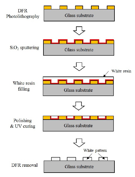
In this study we report how to fabricate fine patterns with reflective white resin by using a dry-film resist (DFR) that serves as an intermediate mold pattern for the resin. The DFRs are supplied with thicknesses of 50 μm and 75 μm, so it is possible to manufacture patterns as thick as 100 μm by accumulating two or more layers. The DFR pattern serves as an intermediate transfer mold for the white resin that is filled in the pattern.[8]
The UV-curing white resin SPI-707, originally designed for fabricating reflective patterns several hundred microns in width for LEDs, was used as the white reflective layer. The recommended thickness was about 13-25 μm. [9] It is very difficult to fabricate patterns thicker than 25 μm because of the low viscosity of SPI-707. The reflective white pattern used in the high efficiency LCDs requires the thickness of the white resin to be more than 50 μm, to ensure high reflectivity. TiO2 beads of diameter 500 nm were added to the white resin, to increase its viscosity and reflectivity.
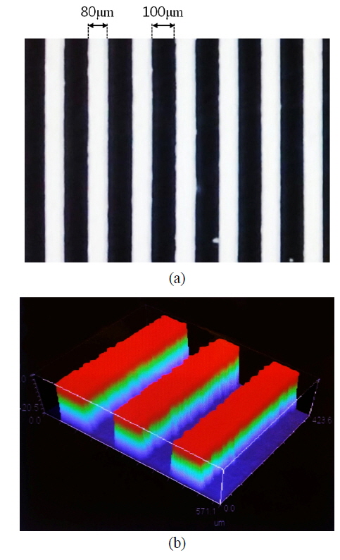
Two reverse-mask patterns were prepared for fabrication of the reflective white patterns. One was a simple mask consisting of an array of linear bars of width 80 μm and pitch 180 μm, as shown in Fig. 3(a), and the other mask included two different patterns of linear bars of widths 30 and 150 μm, the latter containing rectangular apertures of dimensions 100 μm × 130 μm, as shown in Fig. 4. The entire mask was 4 inches across diagonally.
The DuPont negative DFR WBR-2075 of thickness 75 μm was used to produce the reverse pattern on glass of thickness 0.5 mm. First the DFR film was laminated on the glass plate, and then soft baking, exposure, post-exposure baking, development, and washing processes were followed. The laminating process was performed at 95℃ with a speed of 15 rpm, and the soft baking was done at 65℃ for 20 min on a hot plate. The exposure and post-exposure processes were performed at 330 mJ/cm2 and 85℃ for 15 minutes in an oven, respectively. The development was carried out in a 1 wt % aqueous solution of CaCO3 for three minutes.
Figure 2 shows the procedures for fabricating the white pattern, using the DFR pattern as the intermediate mold pattern. Direct application of the UV white resin to the DFR pattern induced a chemical change in the DFR film, due to the strong reactivity of the radical molecules in the UV white resin, so removing the DFR pattern using the DFR remover EKC-162 was impossible. It seemed that the UV exposure and post-exposure baking of the DFR pattern did not induce polymerization strong enough to resist the invasion of radicals included in the UV-curing white resin. To protect the DFR pattern from the attack of radicals, an SiO2 layer about 20 nm thick was sputtered onto the DFR pattern. Then the white resin was applied uniformly on the DFR pattern using a silicone squeezer, and the sample was placed in the UV chamber under 300 mW/cm2 irradiation for 60 seconds. Finally, the SiO2 layer on top of the DFR film was removed by polishing, and the intermediate DFR pattern was removed using the DFR remover EKC-162, leaving the reflective white pattern on the glass panel.
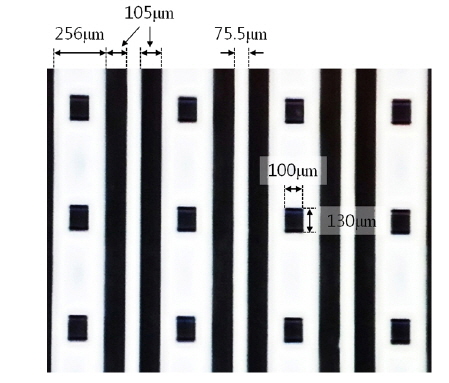
Figures 3 (a) and (b) show the reflective white pattern of width 80 μm and pitch 180 μm and its three=dimensional pattern shape, measured by the WYKO white-light interferometer. The thickness of the white pattern was 46.5 μm, which is less than the DFR thickness of 75 μm, due to the polishing process. The thickness of the white pattern is slightly less than 50 μm, yet much larger than the appropriate thickness of 25 μm specified in the data sheet, and still good enough for high reflectivity. Figure 4 shows a second reflective white pattern consisting of linear white bars of width 75.5 μm plus linear white bars of width 256 μm containing rectangular apertures 100 μm wide × 130 μm high. The rectangular apertures are introduced to reduce the strong blue light, because a large pixel width for blue light transmitted too much light, which deteriorated the white balance. It is shown that the white pattern of width 75.5 μm and height 46 μm and the rectangular apertures were produced quite well.
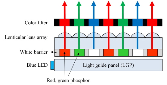
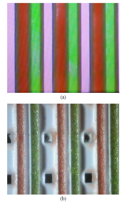
Figure 5 shows white patterns filled with red and green phosphors between the white bar patterns, which can be used as an efficient color-conversion device. The filling with phosphors was performed by a dispenser with nozzle diameter of 100 μm. When the white bar pattern shown in Fig. 3(a), with an aperture fill factor of 55.6%, was placed just above the LED array of the backlight unit, the total transmittance of the linear bar white pattern was measured to be about 92%. This value shows that the recycling of LED light between the reflective white bar pattern and the reflector beneath the LED produced most of the LED light through the open apertures between the white bar patterns.
It is shown in this paper that reflective white patterns tens of microns in size, which are very difficult to fabricate due to the reflection and scattering of light by the particles included in the white resin, can be fabricated quite well using DFR film as an intermediate mold pattern. We tried various methods, including PDMS mold-transfer technology, and found that they are not adequate for white patterns including transparent regions, because most mold-transfer technology leaves residual thin white layers on the transparent regions. Also, it should be possible to fabricate a threedimensional white patternas thick as as 100 μm by using the accumulated DFR film as the intermediate layer. White patterns with high reflectivity will be useful as key optical components in ultraslim direct-lit LCDs, or in the colorconversion device that is needed in a color-matching display.