A one-step fabrication of a photonic crystal (PC) with functional defects is demonstrated. Using multi-beam phase-controlled holographic lithography with a diffracting optical element, large area one dimensional (1D) and two dimensional (2D) PCs with periodic defects were fabricated. The uniform area is up to 2 mm2, and tens of defect channels have been introduced in the 1D and 2D PC structure. This technique gives rise to substantial reduction in the fabrication complexity and significant improvement in the spatial accuracy of introducing functional defects in photonic crystals. This method can also be used to design and fabricate three dimensional (3D) PCs with periodic defects.
Photonic crystals (PCs), proposed in 1987 [1, 2], have undergone rapid development in recent years. Fabrication of 3D PCs was a great challenge over the past decades. Several techniques have succeeded to a certain degree in fabricating 3D PCs. These techniques include e-beam lithography for multilayer stacking of woodpile structures [3], colloidal self-assembly [4], multi-photon direct laser writing [5], and holographic lithography (HL) based on multiple beam interference [6-8]. Using HL to make PCs is one of the most promising techniques for mass production of large area, defect free PC structures. The pattern can be controlled by the beam propagation direction, the number of the interfering beams, the beam intensities, their respective polarizations and relative phases [9]. So far holographic lithography has been successful in fabricating large area, high quality PCs templates [6, 7]. Since the applications of PCs usually require accurate introduction of defects into the PCs’ structure, developing a method to effectively and accurately incorporate functional defects directly into PCs is necessary [10-12]. One way is directly writing by femtosecond laser after the crystal has already been formed [10]. However, this technique requires a costly and complicated second step and an accuracy aligning to the manufacturing process [10]. In 2004, the phase-control holographic lithography was used to introduce defects in a single step [13]. This technique is based on multi-beam diffraction with a phase mask, whose pixels should be much smaller than the period of the PCs, and thousands of pixels are required. Since the smallest pixel of the controlled phase mask is about 1 μm, the period of the fabricated PCs is larger than a few μm by using this technique. Recently, we developed a novel method to introduce defects into the PCs using one-step holographic lithography [14]. A liquid crystal spatial light modulator (LC-SLM) was used to control the phases of interference beamlets. This technique is based on multi-beam interference, the pixel of SLM can be very large (up to 1~2 mm), and ten pixels are enough to fabricate a photonic crystal structure with defects. However, as a lens had been used to focus the interference beams, the interference area was quite small and not uniform. The uniform area is about 500 μm2 and only one defect could be fabricated in the PC structure. To solve this problem, a lens array was used to expand the interference region. [15] Unfortunately, a lens array is a multi-optical-axis system. It is quite difficult to avoid aberrations due to the unparallel optical axes and to the defects of small lenses. In this report, by introducing a diffraction optical element (DOE) and an LC-SLM, large area PCs with periodic defects have been fabricated. Since it is a single optical axis system, the aberrations due to multi-optical-axes can be avoided. Furthermore, using this method a large variety of complex optical structures can be fabricated, such as 3D PCs with periodic defects, quasicrystals [16, 17] and functional metamaterials [18]. This technique will be very useful in the manufacturing of the integrated optics devices.
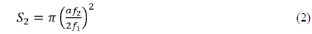
In Ref. 14, in order to form the interference pattern, a lens was used to make the parallel beamlets overlap in the interference area. As a result of the tight focusing, the interference area is limited. The area of tight focusing can be calculated by the equation [19]:

Where,
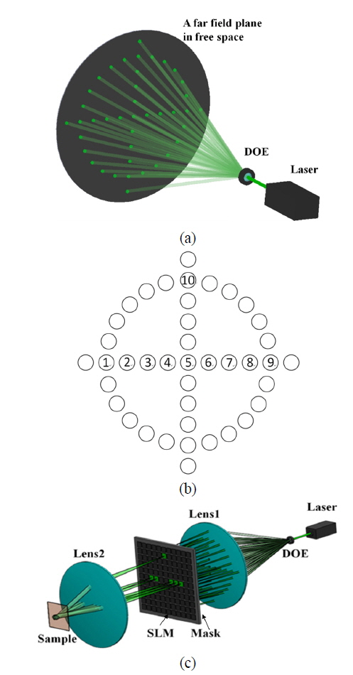
To avoid the tight focusing limitation, a DOE was used in our experiment to expand the interference area. The optical setup is schematically illustrated in Fig. 1. The laser beam was diffracted into several beamlets in different directions by the DOE (DE-R 261 from HOLOEYE Corporation). Figure 1 (a) shows the diffracted beamlets of the DOE. The DOE is similar to a photon’s router, functionally. The diffracted beamlets propagated along different directions and kept the same profile of wavefront as the incident laser beam (similar to a plane wave). In the far field area behind the DOE, the illumination of these beamlets on the plane normal to the optical axis will form a cross-circle dot pattern, shown as Fig. 1 (b). The DOE was designed to make the intensity of the off-axis spots equal and uniform. The diffraction efficiency of the off-axis spots is about 2.1%. To fabricate different PC structures, different DOEs should be carefully designed. 1D, 2D and 3D PC structures can be fabricated by using this DOE.
The optical setup is schematically illustrated in Fig. 1(c). The laser beam was diffracted by the DOE into several beamlets in different directions. Lens1 was used to focus the diffracted beamlets onto different SLM pixels, which were used to precisely control the phase of the interference beamlets. A mask was inserted close before the SLM to select useful beamlets for multi-beam interference. The modified beamlets were collimated by Lens2 as parallel beams in a different direction and overlap near the back focus of Lens2 to make a large interference pattern.
In this optical setup, the back focus of Lens1 and the front focus of Lens2 are superposed, this arrangement constituted a telescope system. The wavefront of diffracted beamlets are the same as the incident laser (similar to a plane wave). After passing through Lens1 and Lens2, the interference beamlets are still similar to plane waves. This setup can avoid the tight focusing limitation. The uniform area of the interference pattern is limited by the beam size of the interference beams. The beam size of the interference beams is given by:
Where,
A photoresist coated on glass substrate was used to record the interference pattern. The photoresist is the resin Epon-SU8 (from Shell) dissolved in γ-butyrolactone (from Aldrich) with 2 wt. % Irgacure 261 (from Ciba. Co.) acting as cationic photoinitiator. The photoresist solutions were spun onto the glass substrate and the solvent was evaporated by 90–95° hard baking to obtain ~1 μm thick photoresist resin films. A Nd:YVO4 continuous-wave laser at 532 nm was used as the irradiation light source. The power of the laser beam before the DOE was 4 mW. After exposure to the interference pattern for about 20 minutes, another soft bake is necessary to complete the cross-linking of the photoresist. Those unlinked regions, which are exposed by the destructive part of the interference pattern, were washed away first by propyleneglycolmetheylether acetate and then cleaned with acetone, leaving behind a copy of the interfering pattern-linked polymer structure.
Holographic lithography is based on the recording of an intensity pattern produced by multi-beam interference. The interference intensity is given by [20]

With i, j denoting different light beams, and
The configurations to achieve desired 1D or 2D PC structure with periodic line defects were calculated in Ref. 14. As shown in Fig. 1(b), the focus spots of Lens1 were aligned as a cross and a circle. For the 1D PC structure with periodic line defect, beamlets 2, 3, 4, 7, and 8 were selected to form the interference pattern. To form the desired PC structure with periodic line defect, the phases of the beamlets 2, 3, 4, 7, and 8 must be accurately controlled by the SLM after the mask. The phases of these five beamlets were {π, 0, 0, π, 0} respectively.
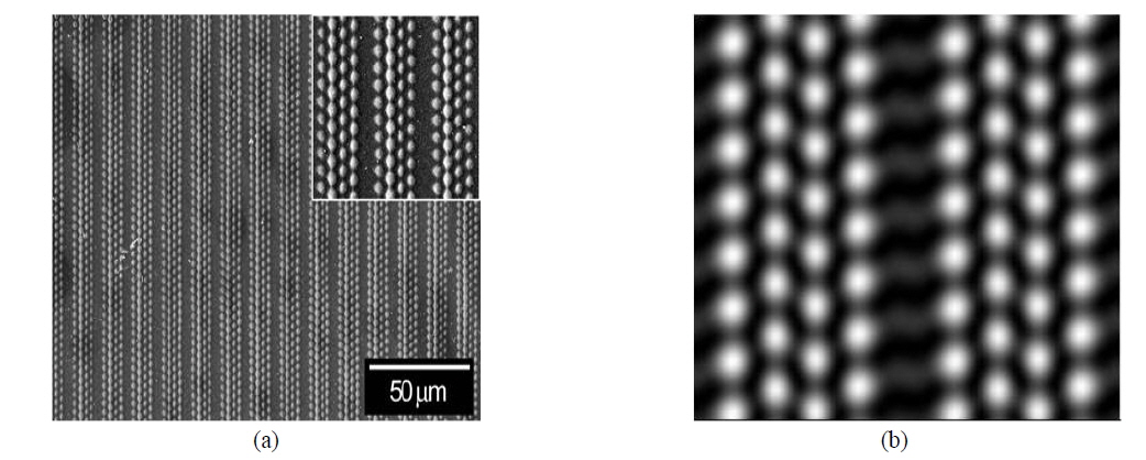
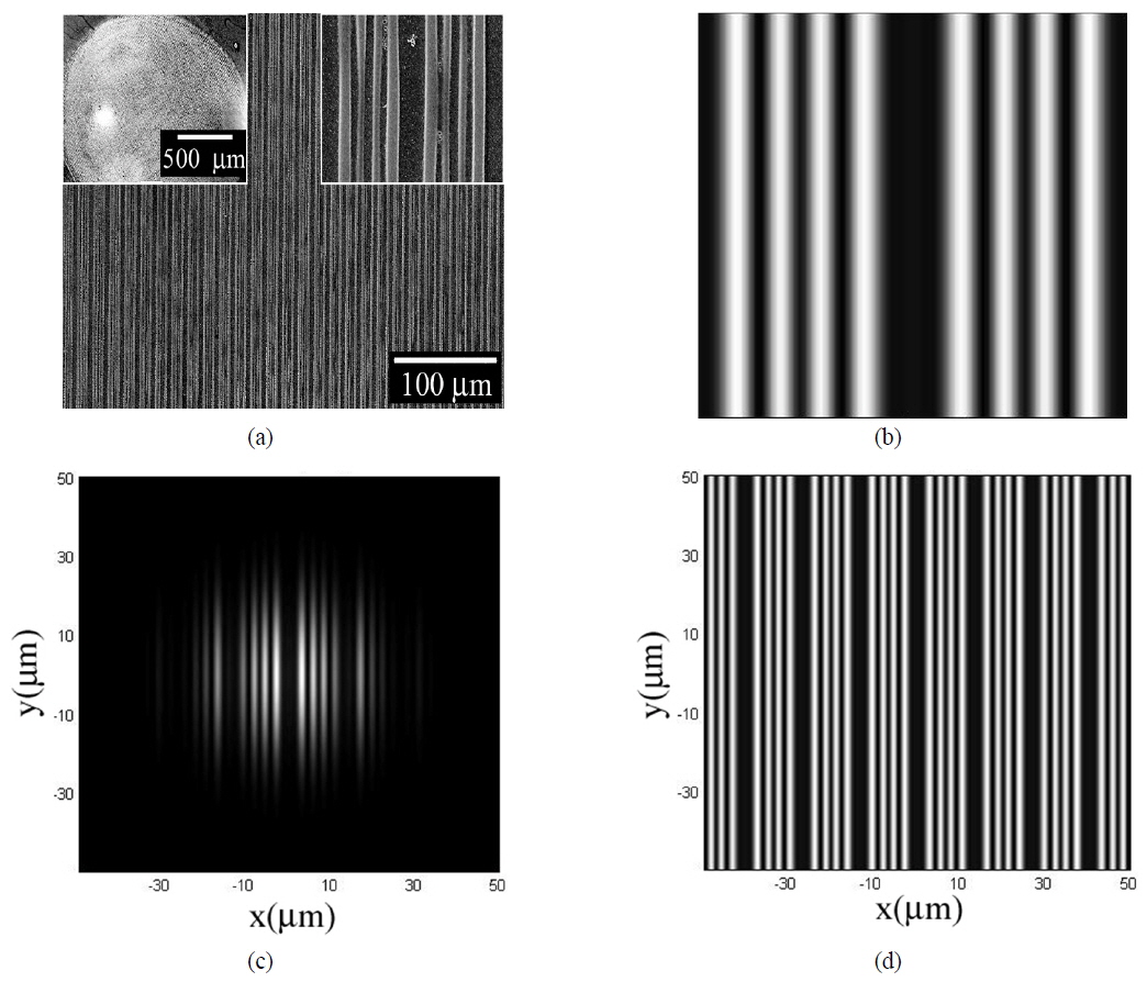
Figure 2 (a) shows the scanning electron micrograph (SEM) image of a 1D sample with periodic line defects. Top-left inset shows that the uniform area of the 1D sample is up to 2 mm2. It shows good agreement with the simulation results. Top-right inset is close-up of the sample. Figure 2(b) shows the computer simulation interference pattern of the optical configuration to fabricate 1D PC structure with periodic defects. The numerical results of 1D PC structure difference between the areas without and with using the DOE setup were shown in Fig. 2 (c) and (d). Therefore, a homogeneous periodical intensity distribution with a large area is obtainable with the use of the DOE.
If additional beamlet 10 is introduced into the optical configuration of 1D PCs with periodic line defects, a 2D hexagonal PC with periodic line defects can be fabricated. Figure 3 (a) shows the SEM image of 2D sample with periodic line defects. Top-right inset is a close-up of the sample. Figure 3(b) shows the computer simulation interference pattern of the optical configuration to fabricate 2D PC structure with periodic defects. A large area, high quality 1D and 2D PC structure with periodic defects were shown in this SEM image, and it is in good agreement with the computer simulation. The uniform area is up to 2 mm2, and about one hundred defects had been introduced in the 1D and 2D PC structures. A negative photoresist was used in this experiment, so that the 2D PC structure is periodic dielectric pillars with air line defects. By using a positive photoresist, the PC structure will be periodic holes with waveguides, which is useful in the semiconductor process.
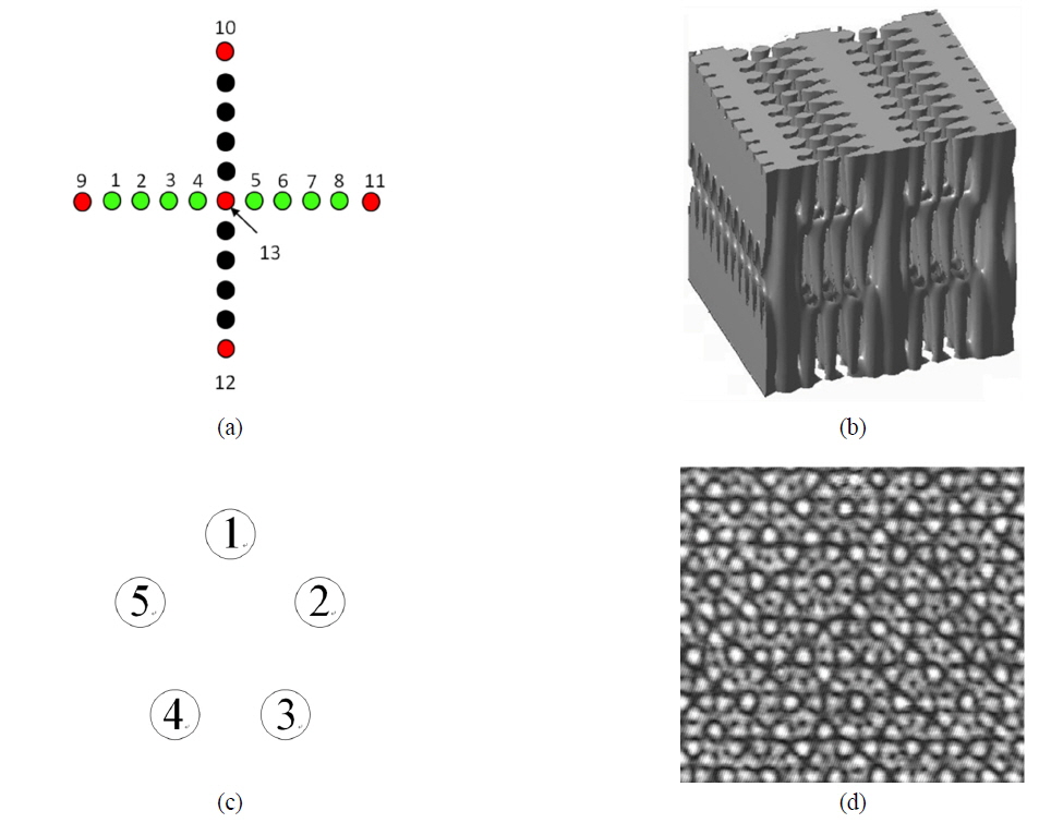
By using this method 3D body-centred-cubic-type (BBC-type) PCs with periodic plane defects can also be fabricated with thirteen phase-controlled beams interference. Figure 4 (a) shows the focus spots pattern of Lens1.
The focus spots were aligned as a cross. At the first exposure, the beamlets 9, 10, 11, 12, and 13 were selected to form the BBC-type PCs pattern. The phases of these five beamlets are {0, 180°, 180°, 270°, 90°} respectively. The beamlets 1 to 8 were used to form the periodic plane defects in the second exposure. The phases of these eight beamlets are {0, 0, 0, 0, 0, 0, 0, 0} respectively. Figure 4 (b) shows the simulation of the interference pattern. Furthermore, by using 5 symmetric interference beamlets, a quasicrystal with 5-fold symmetry can also be fabricated. Figure 4 (c) shows beams configuration to form a quasicrystal with 5-fold symmetry, these 5 focus spots aligned as a regular pentagon. The phases of these 5 beamlets are {0, 0, 0, 0, 0}. Figure 4 (d) is the interference quasicrystal pattern captured by Charge Coupled Device.
To summarize, by applying a simple DOE and an LC-SLM in the optical configuration, we have successfully fabricated 1D, 2D PC structures with periodic defects. The uniform interference area is expanded from 500 μm2 to 2 mm2, and tens of defects embedded into the intrinsic PC structure. This technique gives rise to a substantial reduction of the fabrication complexity and a significant improvement on the accuracy of the functional defects in photonic crystals. We also demonstrated that by using this method 3D PC structure with periodic defects and quasicrystal can be formed. Furthermore, this holographic technique may provide a roadway to fabricate various complex optical structures such as quasicrystals and functional metamaterials.