The RF transceiver for a wireless communication system transmits data through the air with high output power to cover long distances. The transmitter should have high linearity to maintain the high quality of the user data and high efficiency for long battery life. Because the power amplifier (PA) is the most power-consuming component in the transmitter, a highly efficient and linear PA is indispensable for providing seamless, high-quality voice/data/streaming services. In addition, as modern mobile communication standards evolve, a number of PAs are required to cover the various coexisting standards in broadband frequency allocation. A multi-power mode function to control the output power level is necessary to prolong the life of the battery. The wireless industry has been pushing for a singlechip wireless transceiver to achieve low manufacturing cost, small footprint, and multimode/multiband operation capabilities.
Moreover, modern mobile communication standards employ complex spectrally efficient modulation methods. The quadrature phase shift keying (QPSK) and multi-level quadrature amplitude modulation (M-QAM), as a combination of phase shift keying and amplitude shift keying, and orthogonal frequency division multiplexing (OFDM) are used in modulation in order to transmit a great deal of information in a limited spectrum resource. The modulated signals result in a non-constant envelope signal with a wide channel bandwidth and a high peak-to-average power ratio (PAPR) for the input of the PA. As a result, a PA should amplify the signals in the back-off power regions, where the efficiency of the PA is inherently extremely low because of the fixed supply voltage and the optimized load impedance at peak instantaneous power. In addition, the output power, efficiency, and linearity of PAs degrade dramatically as the signal bandwidth and/or operation frequency increases because the sideband asymmetry of PAs generated by memory effects is directly proportional to the channel bandwidth.
The requirements of PAs for modern wireless communication systems are high output power, high linearity, high efficiency, high level of integration, and multimode/multiband operation capabilities. The most promising solution to meet these demands is making the PA using a CMOS process. Furthermore, as the PA is co-integrated with other portions of the transceiver fabricated in the CMOS process, significant performance improvement can be achieved by utilizing baseband signal processing and Si-based on-chip linearization techniques [1-11]. However, it is challenging to integrate the PA into CMOS technology when the other blocks of the transceiver are already integrated. CMOS devices have several disadvantages impeding the realization of a PA, such as low breakdown voltage, low-current-driving capability, high knee voltage, low quality factor in the passive component, and lossy silicon substrates. Therefore, performance improvement techniques are required to overcome the inferior characteristics of CMOS devices.
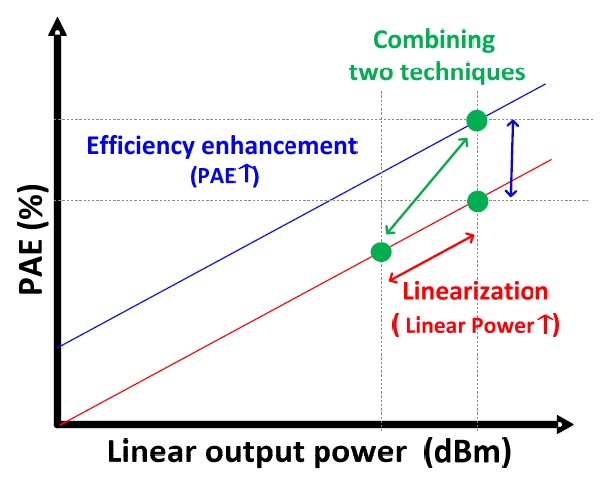
In this paper, two approaches for improving the performance of a CMOS PA are exploited for linearization and efficiency enhancement, as shown in Fig. 1. It is difficult to improve linearity and efficiency simultaneously due to their trade-off relationship. The linearization technique improves the linear output power and provides higher efficiency. The purpose of the efficiency enhancement technique is to enhance efficiency without degrading the linear output power. Hence, applying both techniques to a CMOS PA is a practical solution for accomplishing our goal.
The performance of a PA is strongly dependent on its bias conditions, hence, integrated bias circuits can be utilized for linearization, which is one of the advantages of the CMOS process. For high linearity and efficiency, PAs with a deep class-AB operation are the most attractive [12]. However, a deep class-AB PA with a bias near the threshold voltage generates a large inter-modulation distortion (IMD) at the low- and midpower regions, and it has a strong gain-expansion characteristic that degrades the AM-AM [13,14]. The adaptive bias circuit can suppress the distortion and gain deviation. Additionally, injecting a proper envelope signal through a bias circuit at the input of a PA reduces the IMD components at a high power region, canceling any distortion [15-19]. The gain of the PA is expanded at the saturated region when the envelope signal is injected at the gate, compensating the gain compression. Therefore, the performance of a PA can be further improved by the collaboration of the two adaptive bias circuits.
The use of a high PAPR signal reduces the efficiency of PAs because the supply voltage provided to the PAs is fixed and the output load is optimized only for the peak instantaneous power. To improve the efficiency for the high PAPR signals, envelope tracking (ET) techniques effectively modulate the supply voltage of the PA according to the instantaneous output power. To simultaneously achieve wideband and high efficiency operation, a hybrid switching supply modulator, which is composed of a linear regulator and a switching mode power supply (SMPS), is commonly used [20-26]. Integrating the PA and the supply modulator on the same die is possible using a CMOS process. The ET technique is also well-suited for multimode/multiband operation because the multimode is handled by the supply modulator and the multiband is handled by the broadband PA itself.
The organization of this paper is as follows. Section II describes the standard design of a CMOS PA with saturated waveform engineering for efficiency improvement. Section III shows linearization techniques for a CMOS PA. Section IV focuses on a CMOS ET PA with dynamic auxiliary circuits for optimized ET operation.
II. HIGH-EFFICIENCY DIFFERENTIAL CASCODE CMOS PA DESIGN
In the CMOS process, a differential cascode structure PA is widely used to minimize the source grounding problem of a common-source (CS) amplifier and to enhance the breakdown voltage. Because of the low transconductance of CMOS devices, large power cells are required to achieve high output power. Parasitic components due to the large cells can lead to degradation of the efficiency and linearity of the PA. Because the differential structure doubles the voltage swing to a balanced load, the load impedance can be four times larger. For the same load impedance, the output power can be two times larger than that of a single-ended structure. Hence, the use of a differential structure helps to mitigate the drawback of the power generation problem. In this chap ter, based on two basic structural concepts for a CMOS PA design, the differential cascode structure and saturated waveform engineering are introduced.
1. Differential Cascode Structure
For a CMOS process, a differential cascode structure is widely used to reduce the degeneration effect of bonding wires at the source of the CS amplifier. A feedback loop connected between the gate of the CS and the drain of the common-gate (CG) can improve stability and linearity [27]. An output transformer is employed to convert the differential output into a single-ended one and combine the two output powers. However, the overall efficiency is degraded due to the insertion loss of the transformer.
The common nodes of the differential structure create virtual grounds for odd harmonics and open for even harmonics. The common node voltage of the gate of the CG stage at the second harmonic is not properly terminated because of the bias network, which includes bonding wires and resistors. Furthermore, the common node voltage of the CS stage at the second harmonic is not properly grounded and degrades the overall performance. The second harmonics cause memory effect and degrade the linearity. Therefore, proper grounding for the second harmonic is essential for improved linearity. Employing a second harmonic control circuit at the gate of the CG and the source of the CS stages as proposed in [27] and [28], these second harmonic components can be eliminated, thereby reducing the mixing of the second-order products to IMD and improving the linearity.
The differential structure requires a differential to singleended mode conversion. Moreover, to realize high output power, an impedance transformation output network is needed to lower the load from 50 Ω to the optimum impedance. These can be covered by the transformer; it functions simultaneously as an impedance transformer and a power combiner. The insertion loss of the output power combiner in a differential structure is mainly dependent on the quality factor of the material used. A transformer based on a bulk CMOS process experiences a large loss due to the conductive substrate and thin-metal layer. To reduce such loss, an offchip transformer can be used. Off-chip transformers are designed on an integrated passive device (IPD) [18] or a printed circuit board (PCB) [29,30]. A transmission-line transformer (TLT) transmits the energy from the input to the output by a coupled transmission line mode and not by flux-leakage as in a conventional transformer. A TLT exhibits broadband characteristics, making it easier to design a broadband PA [27].
3. Saturated Waveform Engineering for CMOS PAs
The minimum voltage swing of the PA is limited by the knee voltage. This degrades the efficiency, linearity, and output power. Unfortunately the knee voltage of a cascode structure is higher than that of a CS-based structure. To reduce the knee voltage, a CG device is usually larger than a CS device. The parasitic components of the CG device, including the nonlinear Cout, also increase proportionally. The size of the CG device needs to be selected carefully, because the self-generated harmonics from the nonlinear Cout can deteriorate the efficiency and linearity [31].
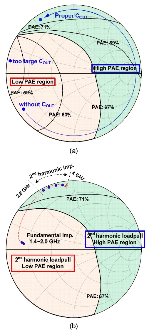
The saturated waveform engineering of the CMOS PA has been analyzed and implemented in previous work [32]. The harmonic components from the nonlinear Cout are tuned based on load-pull simulation and waveform engineering. The second harmonic is the key element and the third harmonic can provide assistance for the saturated waveform engineering. A second peaked half-sinusoidal voltage waveform with an increased fundamental voltage component should be made for the saturated waveform. To generate this voltage waveform, an in-phase second harmonic is required and it is generated by the nonlinear Cout. The higher peak voltage swing within the possible breakdown voltage range is advantageous for improving the efficiency and output power, especially for cascode structure having large knee voltages.
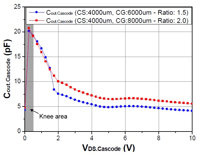
Based on the analysis of saturated waveform and load-pull data, the optimized Cout can be found for highly efficient operation of the saturated PA, as shown in Fig. 2(a). As previously mentioned, Cout can be adjusted by selecting the proper size of CG device. The size of the CG device (6,000 m) is chosen to be 1.5 times larger than that of the CS device (4,000 m). As shown in Fig. 3, the nonlinear Cout of the 6,000 m (1.5 ratio) device is reduced by 36% compared to that of the 8,000 m device (2.0 ratio). The peak drain-source voltage (
III. CMOS PA WITH LINEARIZATION
1. Linearization Techniques Using an Adaptive Bias Circuit
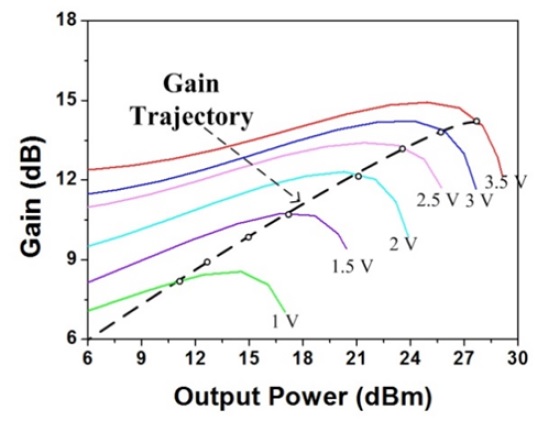
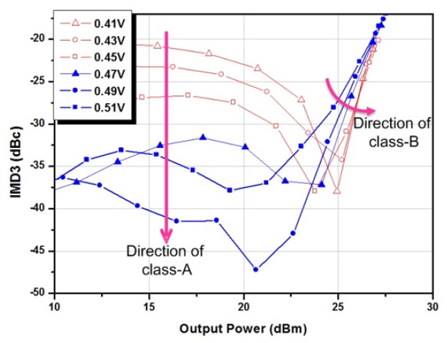
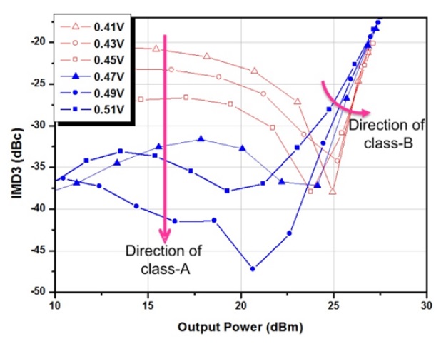
The overall performance of a PA is strongly dependent on its operation class, which is determined by the gate bias. Generally, a deep class-AB mode with a low quiescent-current operates more efficiently than that with class-AB or class-A modes at a high-power region. For small signal operation with a deep class-AB mode, linearity degrades compared to the class-A mode. However, for the case of a large signal operation, internal harmonic cancelation improves the linearity at the high-power region by forming a sweet-spot. Therefore, a deep class-AB mode operates more efficiently and linearly than operations with class-AB or class-A modes at a high power region because the IMD minimum point (sweet-spot) moves toward the compression point, as shown in Fig. 4. Therefore, a deep class-AB operation is the most attractive operation for a linear PA design at a high-power region. However, as shown in Fig. 4, linearity at low- and mid-power regions degrades severely as bias voltage moves toward class-B. This is due to the severe nonlinear behavior at or near the turn-on voltage of the deep class-AB operation, which generates a large distortion.
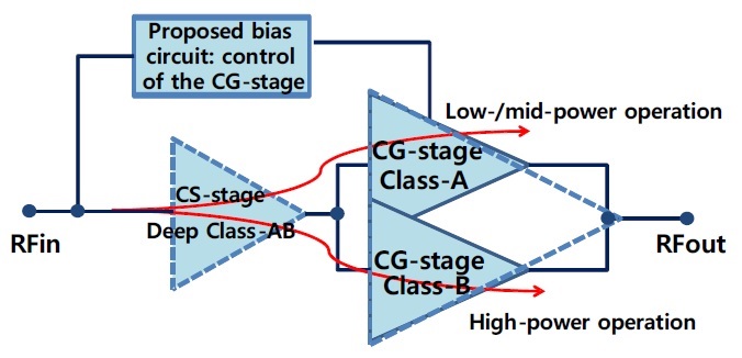
A differential cascode amplifier is composed of CS and CG amplifiers. The CS functions as a main amplifier and the CG amplifier functions as a current buffer. Combining a gain-expansion stage (deep class-AB) and a gain-compression stage (class-A) can compensate the AM-AM distortion. Examples of this are MGTR and multi-stage cascade structures [33,34]. Fig. 5 shows a block diagram of the linearization process. The CS stage operates in deep class-AB mode for high efficiency and linearity, while the CG stage operates in either class-A or class-B mode, according to the input power level, to compensate the nonlinear distortion generated by the CS stage. That is, for high performance cascode PAs, the gate bias of the CG device should be properly controlled. Fig. 6 shows the simulation results of the gain and IMD3 for a two-tone signal with 10-MHz tone spacing at a 1.85-GHz center frequency. To see the effect of the gate bias of the CG device, the gate bias of the CS is fixed to a deep class-AB bias (0.46 V) and the CG is varied.
As plotted in Fig. 6, the gain and IMD3 can be adjusted using the gate bias of the CG device. The gain deviation reduces with higher gate voltage, reducing the AM-AM distortion. IMD3 behavior is quite similar to the CS device. At the low- and mid-power regions, the IMD3 is low with a high gate bias, and for the high power region, over 23-dBm in our design, the gate bias should be low to achieve better linearity. Knowing this behavior, we can find the optimum gate bias for the CG device to minimize the AM-AM distortion and improve linearity. Fig. 7 plots the optimumgate bias of the CG device along with the output power. By this reshaped gate bias, the gain deviation and IMD3 are simultaneously improved by 2 dB and 6 dB, respectively, as shown in Fig. 8.
Therefore, we use this optimally shaped CG bias to improve the linearity and gain deviation at the low-power region, while the CS device operated in a deep class-AB bias to achieve better performance at the high-power region. We previously reported the measured adjacent channel leakage ratio (ACLR), gain, and PAE with a reshaped CG gate bias [27,35]. For a 10-MHz bandwidth LTE signal at 1.85 GHz, the PA with the proposed bias circuit improves E-UT-RAACLR from 7.0 dB to 2.5 dB over the constant bias. The PA with the CG bias shows a significant improvement in ACLR, which is affected by the reduction of the AM-AM distortion and IMD3.
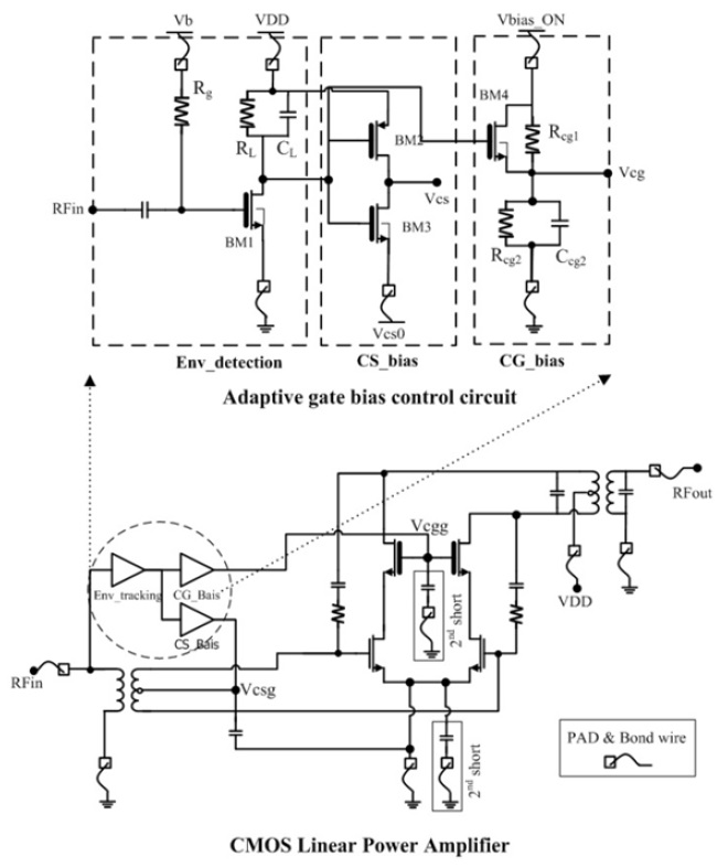
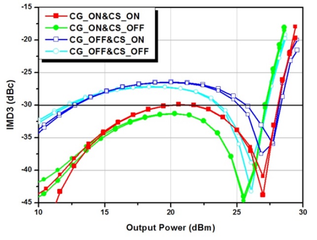
For further improvement of linearity at the high-power region, an envelope signal injection to the gate of the CS stage can be used [36,37]. The envelope injection technique is adopted using a class-D bias circuit [18,27]. Fig. 9 clearly shows the effect of both linearization techniques on the CS and CG devices. The envelope injection at the CS improves high-power linearity while the optimal reshaped gate bias at the CG improves linearity at the low- and mid-power regions. Both bias circuits are merged into one circuit to simplify the circuitry. A CMOS PA schematic with adaptive gate bias control circuits is shown in Fig. 10.
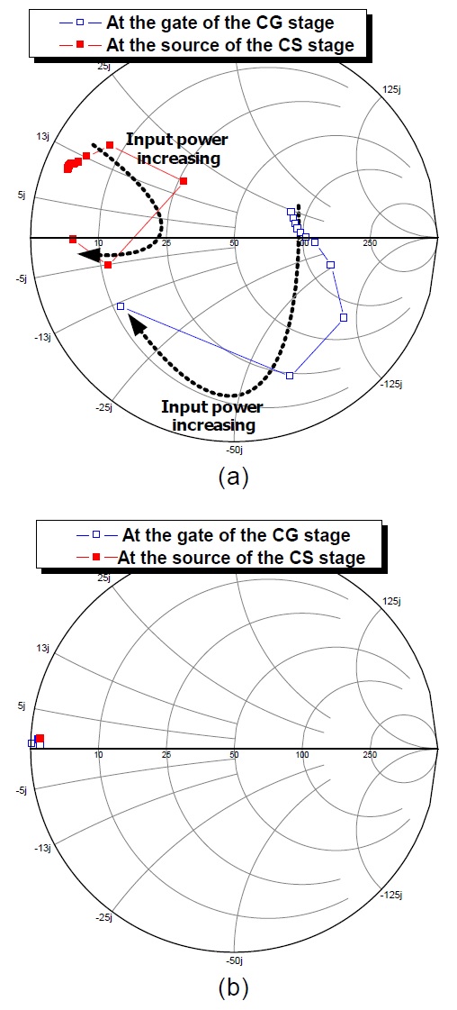
The memory effect is mainly caused by the envelope frequency and second harmonics at the device terminals [38]. Hence, by removing the envelope or second harmonics, we can reduce the sideband asymmetries. To make a short circuit condition at the envelope frequency, a low-pass filter consisting of large capacitors is needed, which is hard to implement in a real device. Therefore, control of the second harmonic impedance is a practical solution for reducing the sideband asymmetries, as proposed in [27] and [28]. A differential cascode amplifier has two common nodes; one at the source of the CS and another at the gate of the CG stage. If the source impedance of the CS stage does not terminate at the second harmonic, the linearity of the amplifier is deteriorated by the series feedback of the impedance. Also the gate impedance of the CG stage, which is a part of the output load seen by the CS stage, should be terminated properly. These terminations allow significant reduction of the memory effects and second-order nonlinear distortions.
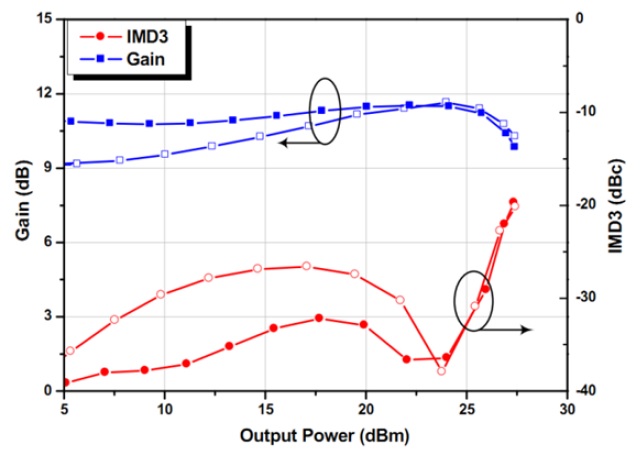
Fig. 11(a) shows the second harmonic impedances at the gate of the CG and the source of the CS stages of the PA according to the input power at a frequency of 1.85 GHz. As shown, neither of the second harmonic impedances is properly shorted. These second harmonic impedances can make the sideband asymmetric and degrade the IMD3. After applying the second harmonic control circuits, the second harmonic impedances at the common nodes are properly terminated to a short-circuit condition, as shown in Fig. 11(b). The second harmonic control circuits are composed of a capacitor and an inductor in series, as shown in Fig. 10.
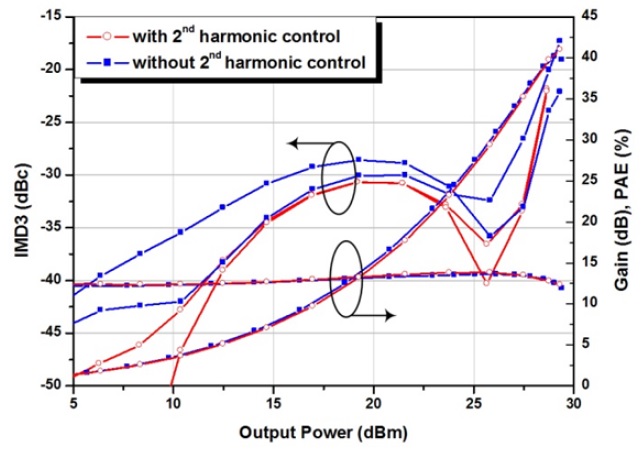
To verify the linearization techniques, a simulation of the IMD3 result using a two-tone input signal with spacing of 10 MHz at a 1.85-GHz center frequency is performed. The simulation result illustrated in Fig. 12 clearly shows that with the second harmonic control circuit, the asymmetry of the IMD3s is reduced and linearity is improved. The second harmonic short suppresses the asymmetry of the wide video band signal [28].
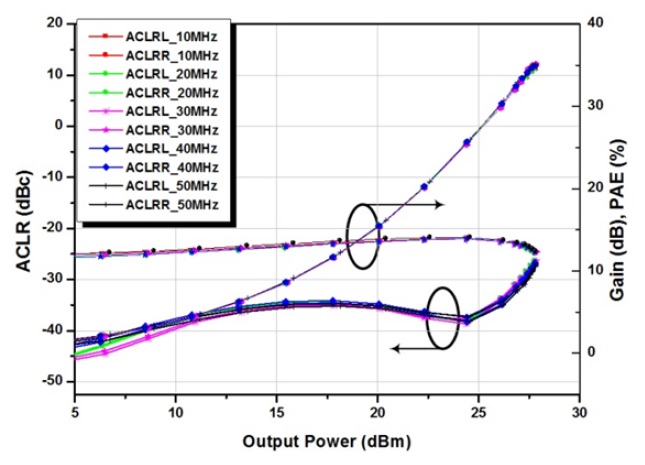
For a demonstration of the wide video band operation, the proposed PA is tested with 10- to 50-MHz bandwidth 16 quadrature amplitude modulation (16-QAM) 7.5-dB PAPR LTE signal at 1.85-GHz. The ACLR is measured under an evolved universal terrestrial radio access (E-UTRA) specification with a 9-MHz resolution bandwidth at both a center frequency and a 10-MHz offset. Fig. 13 shows the measured performance. The PA has an average output power and a PAE of 27.3 dBm and 33.0%–32.7%, respectively, while the E-UTRAACLR level is under -30.5 dBc, as shown in Fig. 13. The performance does not change with the signal bandwidth.
IV. CMOS ENVELOPE TRACKING PA WITH CONTROL
Modern wireless communication systems use complex modulation schemes to handle massive amounts of data. These signals have large PAPRs. ET techniques can be very effective for improving the efficiency of high PAPR signals by modulating the supply voltage according to the instantaneous output power. The efficiency and linearity of an ET PA is strongly dependent on the performance of the supply modulator. To enhance the efficiency of the supply modulator, several techniques, such as a dual-switch and a feed-forward signal, are report in [39-41]. The bandwidth of the supply modulator is enhanced to accurately track the wideband signal without generating distortions [26,42,43]. The envelope shaping methods have been investigated for optimized ET operation [44]. This envelope shaping method, sweet-spot tracking, can provide the best performance for ET-based PAs [29,30,32].
As previously mentioned, a great deal of effort has been concentrated on the ET supply modulator itself. Just applying ET to a conventional PA improves the efficiency and linearity, but further improvement can be made by designing the PA for optimum ET operation. There are, however, several challenges when applying the ET technique to a PA.
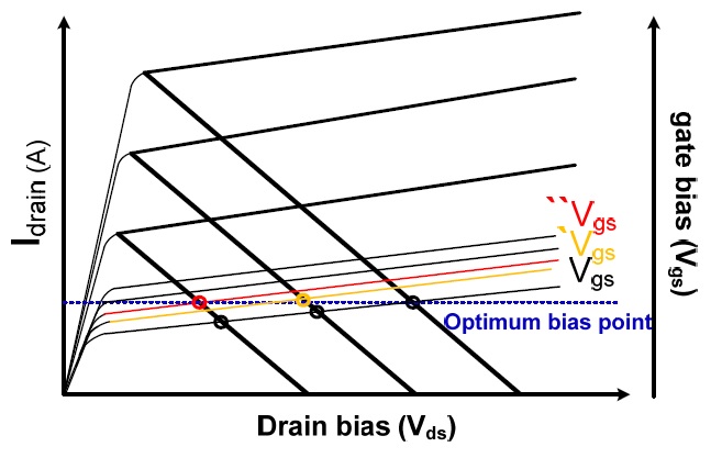
As the drain and gate voltages are changed, the drain current varies with non-constant transconductance (Gm) and nonlinear output capacitance. As a result, a large gain variation is generated under ET operation, as shown in Fig. 14. This can lead to AM/AM distortion and degradation of efficiency and linearity. Fig. 15 shows a DC-IV curve with a load-line under the ET operation. As shown in the two figures, to reduce the AM/AM distortion, the gate bias should be adjusted with the drain bias. For further improvement in AM/AM distortion, dynamic feedback control is proposed [32].
To ensure the saturation operation to the CG device under ET operation, the CG bias should be adjusted. Because the gate of the CG determines the drain bias of the CS stage, the gate must be modulated in the same way as the supply node for optimized ET operation.
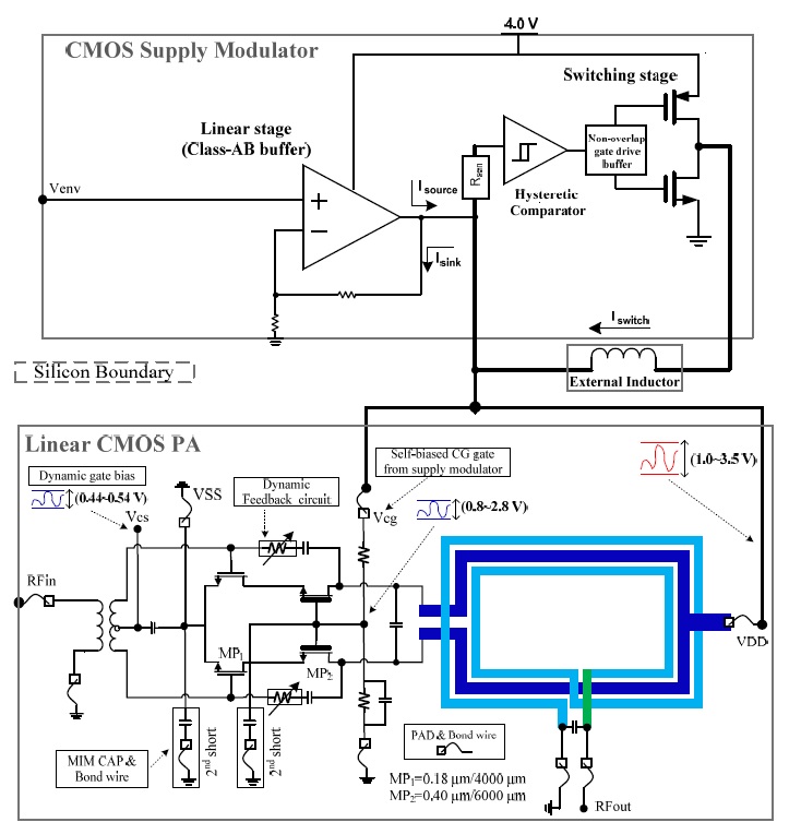
The proposed overall schematic of the CMOS ET PA, including the CMOS saturated PA and supply modulator is shown in Fig. 16. For a high performance ET PA, the PA has adopted the techniques mentioned in the previous sections. Additionally, dynamic auxiliary circuits are employed for optimized ET operation.
1. Dynamic Feedback and Adaptive Gate Biasing of the CS Stage
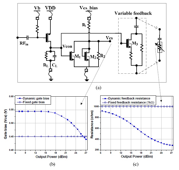
The feedback factor, bias dependent Gm, and output load impedance determine the gain of the CMOS PA. Because the output load impedance is defined by the overall performances, it cannot be employed for tuning the gain. A feedback network is generally used to improve the linearity and stability of the PA, at a cost of the gain. The feedback circuit is composed of a resistor and a capacitor, hence, the gain of the PA can be tuned by controlling the resistance. The gain is also strongly dependent on its gate bias. Therefore, by controlling the feedback circuit and gate bias, the gain of the PA can be tuned.
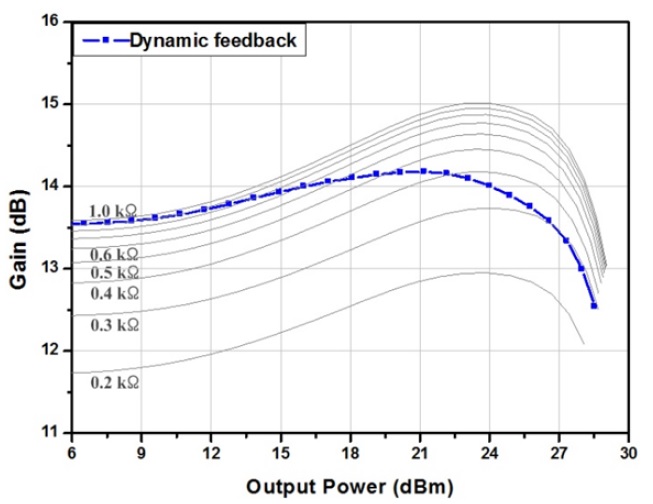
The proposed dynamic feedback and CS gate bias control circuits are shown in Fig. 17(a). The circuits consist of the envelope detector, which amplifies the RF input signal to detect the envelope level, the bias controller for the gate of the CS stage, and a series connected variable resistor and capacitor for dynamic feedback control. The reshaped control ranges of the gate voltage and the feedback resistance are from 0.54 V to 0.44 V and from 0.9 kΩ to 0.3 kΩ, respectively, according to the output power level, as shown in Fig. 17(b) and (c). By applying dynamic feedback control, the maximum gain variation is reduced within 0.5 dB, as shown in Fig. 18.
2. The Self-biased Gate Terminal of the Common-gate Stage
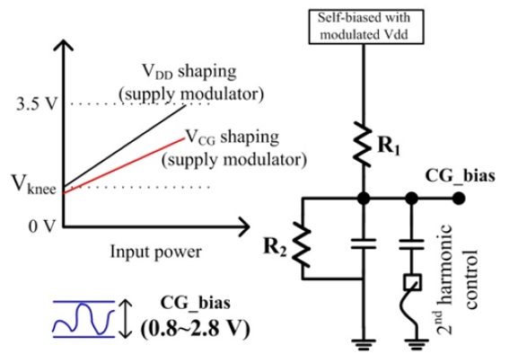
The CG device gets into the triode region when the drain bias is lower than the saturation voltage, generating a large amount of distortion and reducing the dynamic range of the ET operation. In addition, the efficiency of the supply modulator deteriorates when the CG device is operated in the triode region due to the increased on-resistance. To ensure the proper saturated operation of the CG device when applying the modulated supply bias, the gate bias of the CG stage should also be properly modulated in the same way as the drain voltage. The optimum CG bias shaping for improving linearity and efficiency is reported in [45]. We have proposed a simple self-bias circuit for the CG stage shown in Fig. 19. Without using any additional signal processing, the modulated supply voltage is shifted by using a simple resistive divider. The reshaped voltage, 2.8 to 0.8 V, is converted from a modulated supply, 3.5 to 1.0 V. When applying the proposed self-biasing method to the cascode PA with ET operation, the CG device operates in the saturation region for all swing ranges of the modulated supply voltage, thus achieving better linearity and higher efficiency.
3. Verif ication of the Proposed CMOS ET PA with the Auxiliary Circuits
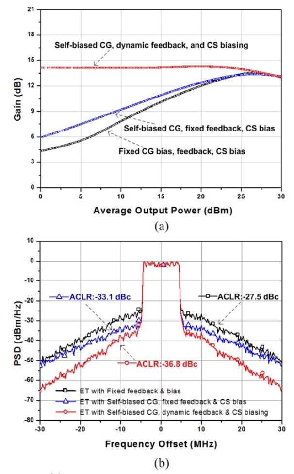
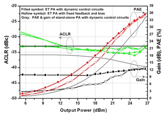
The performance improvements of the ET PA using the proposed techniques were verified by simulating the entire ET PA with the auxiliary circuits. The gain and power spectral density (PSD) were simulated using an LTE 10-MHz BW signal [46]. The gain variation of the proposed ET PA is reduced dramatically compared to the one with fixed biases and feedback ET PA, as shown in Fig. 20(a). As a result, the dynamic range of the ET PA is drastically improved. The output PSD of the ET PA with the proposed auxiliary circuits has lower E-UTRAACLR compared to that with the fixed bias and feedback, as shown in Fig. 20(b).
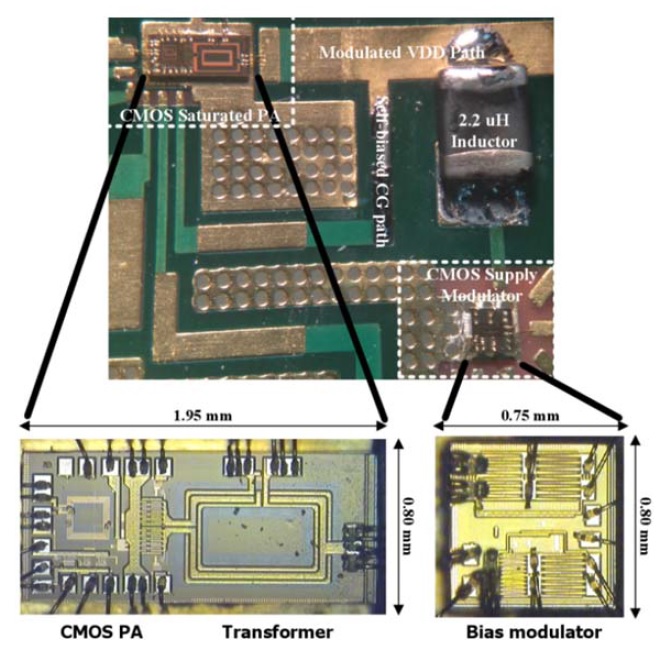
It is worth mentioning that the proposed auxiliary circuit techniques are suitable for improving the performance of ET PAs. Fig. 21 shows a micrograph of the ET PA module, including the fully integrated CMOS saturated PA, supply modulator, and external inductor. The fabricated PA is tested with a 10-MHz bandwidth 16-QAM 7.5-dB PAPR LTE signal. The ACLR is measured under the E-UTRA specification with a 9-MHz channel measurement bandwidth at a 1.85-GHz center frequency and a 10-MHz offset. Fig. 22 shows the measured results. The measured performance is similar to the simulation results, with the proposed auxiliary circuit gain deviation reduced within 1 dB and improved linearity at all average output power ranges.
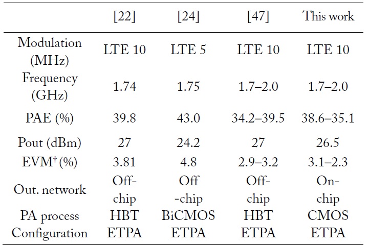
The proposed auxiliary circuits enable the CMOS ET PA to outperform the conventional ET PA and deliver highly linear and efficient performance without using a DPD technique. Table 1 summarizes a comparison of the previously reported results. The proposed PA delivers an advantageous performance despite the fully integrated CMOS circuit.
[Table 1.] Performance comparison with state-of-the-art results

Performance comparison with state-of-the-art results
The CMOS PA is a promising solution for highly-integrated transceivers. However, the implementation of PAs using the CMOS process is a major challenge because of the inferior characteristics of CMOS devices. This paper focused on the improvements of efficiency and linearity of CMOS RF PAs for modern wireless communication systems. With the proposed techniques, the fully integrated CMOS ET PA achieves competitive performance, suitable for employment in real systems.