This paper presents a design of a transmission line negative group delay (NGD) circuit with multiple pole characteristics. By inserting an additional transmission line into a conventional NGD circuit, the proposed circuit provides further design parameters to obtain wideband group delay (GD) and to help reduce signal attenuation. As a result, the number of gain compensating amplifiers can be reduced, which can contribute to stable operation when integrated into RF systems. The multiple pole characteristics can provide wider NGD bandwidth and can be obtained by connecting resonators with slightly different center frequencies separated by quarter-wavelength transmission lines. For experimental validation, an NGD circuit with two poles GD characteristic is designed, simulated, and measured.
Electromagnetic wave propagation in any medium obeys the fundamental physical laws described by Maxwell’s equation [1]. Most media exhibit normal propagation called subluminal, where the speed of propagation of individual timeharmonic components is slower than the speed of light,
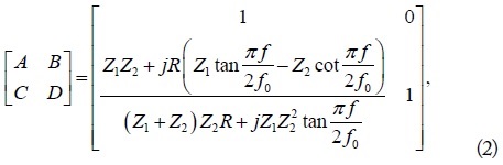
The wave propagation in any medium can be characterized by group velocity and group delay (GD), which are same. The GD in a circuit can be investigated by examining transmission phase variation with respect to frequency and can be defined as a negative derivative of the signal transmission phase according to frequency, as shown in (1).
As seen from (1), when quantity
The negative group delay (NGD) occurs at a certain range of frequency where the absorption or SA is maximum [1]. Therefore, band-stop structures are used to realize NGD circuits. Based on either series or shunt
A few studies have been conducted about NGD networks with small SA. In [13], a composite NGD network with smaller SA was presented. However, this circuit requires parallel lumped elements (such as capacitors and inductors) between two transmission lines, making implementation difficult at microwave frequencies.
In this paper, a design of the transmission line NGD circuit with reduced SA and multiple pole GD characteristics is presented.
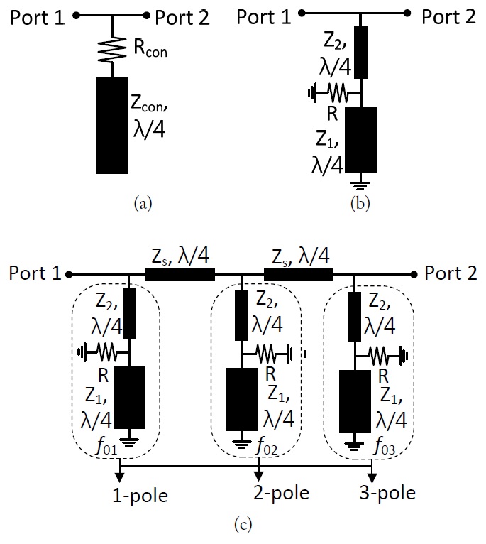
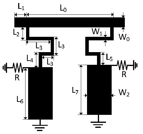
Fig. 1 shows the structure of the conventional and proposed 1-pole NGD circuits that consist of resistor
where

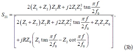
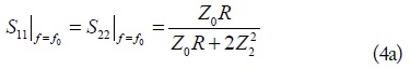
where Z0 is reference port impedance. Furthermore,

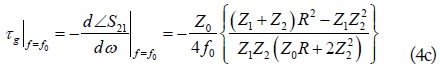
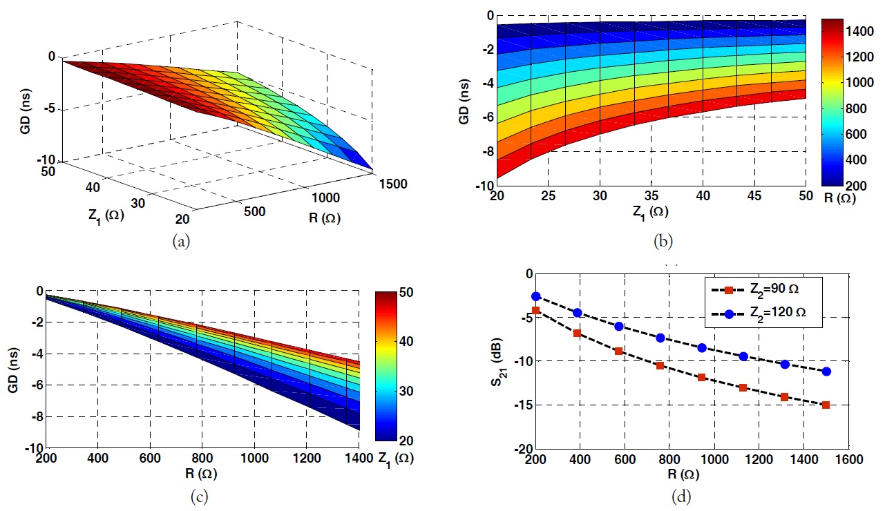
As seen from (4c), the maximum achievable GD depends on Z1, Z2, and
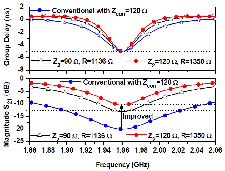
Fig. 3 shows the simulation results of the 1-pole NGD circuit. In this simulation, the maximum achievable GD at
The temperature dependence of
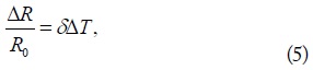
where
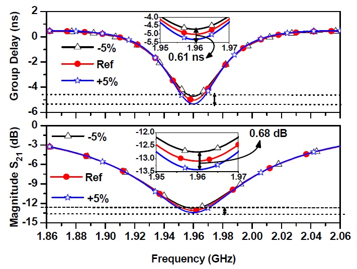
Fig. 4 shows the performance degradation of the proposed 1-pole NGD circuit, assuming the resistance variation of ±5%. As seen from this figure, the GD and SA (magnitude of
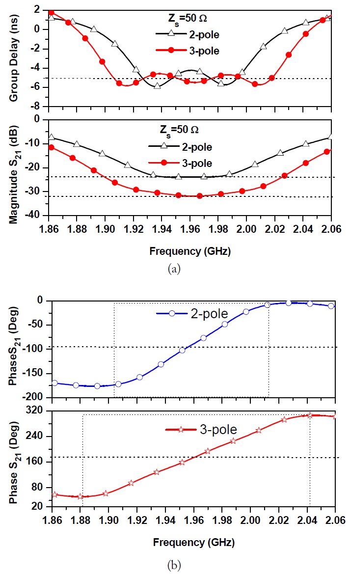
The NGD bandwidth can be enhanced by connecting 1-pole NGD circuits with the slightly different center frequencies (
Fig. 5(a) shows the simulated GD and
III. SIMULATION AND EXPERIMENTAL RESULTS
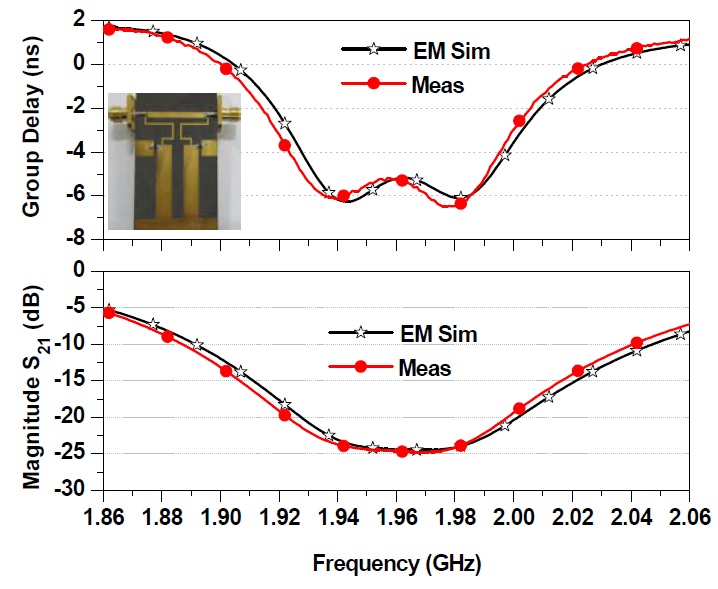
For experimental validation of the proposed circuit, the design goal was to obtain a GD of -6 ns at
[Table 1.] Physical dimensions of the 2-pole negative group delay circuit (unit = mm)
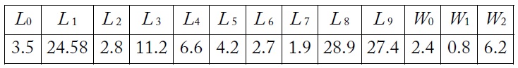
Physical dimensions of the 2-pole negative group delay circuit (unit = mm)
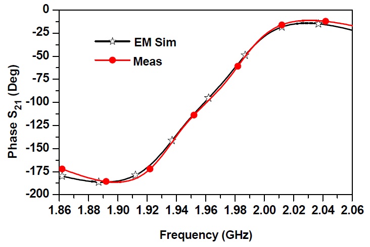
Fig. 7 shows the simulated and measured GD and magnitude results of the 2-pole NGD circuit. From the measurement, the GD was determined as -5.80±0.45 ns over a bandwidth of 80 MHz. The maximum SA at
This paper demonstrates the design of an NGD circuit with multiple pole GD characteristics and reduced signal attenuation. The multiple pole NGD circuit is obtained by the cascade connection of several 1-pole circuits having slightly different frequencies. For the experimental verification, the 2-pole NGD circuit was designed, fabricated, and measured. The proposed topology can reduce the number of gain-compensating amplifier stages and can help improve efficiency, out-of-band noise reduction, and stable operations when integrated into RF/microwave systems.