Effect of silicon doping into ZnSnO systems was investigated using solution process. Addition of silicon was used to suppress oxygen vacancy generation. The transfer characteristics of the device showed threshold voltage shift toward the positive direction with increasing Si content due to the high binding energy of silicon atoms with oxygen. As a result, the carrier concentration was decreased with increasing Si content.
Employment of amorphous oxide semiconductors (AOSs) provides the opportunity to develop superior electrical properties for display technology and other applications. These oxide semiconductors have transparency in the visible region and higher mobility compared with a-Si: H. Among the emerging semiconductor technologies, AOSs have attracted significant attention due to their high functional properties, including high mobility, high flexibility and low-temperature fabrication process. The promising functional materials for high performance thin film transistors (TFTs), such as indium-gallium-zinc oxide (IGZO) and zinc-tin-oxide (ZTO), exhibited high field effect mobility even in the amorphous phase because of the large edgesharing structure of the s-orbitals [1-3]. Thus far, various materials, including Zn-Sn-O (ZTO), In-Zn-O (IZO), and In-Ga-Zn-O (IGZO), have been employed for the fabrication of oxide TFTs, and have been reported to show acceptable device performance for flat panel display (FPD) backplane applications. There are many vacuum synthesis technologies for TFTs, including physical vapor deposition (PVD), chemical vapor deposition (CVD), and pulsed laser deposition (PLD)[4-7]. However, these methods require expensive equipment due to inclusion of the vacuum process, thus resulting in high processing cost. Solution process has many advantages compared to the traditional deposition processes. First, it does not require vacuum processing and can be used for large area deposition. Furthermore, solution processes also allows much variation simply by controlling the compositions of the precursor ratio. Recently, the solution fabrication method was found to be suitable for flexible and large area flat panel displays, because such devices require room temperature processing and large size deposition. In the present study, we demonstrate variation of the threshold voltage of SZTO TFTs with incorporation of Si fabricated using solution process. Si has a lower standard electrode potential (SEP) than those of Sn and Zn, and thus can degenerate oxygen vacancy. [8-9] As a result, Si can act as a carrier suppressor in the SZTO system, and making it possible to control the threshold voltage through variation of the Si content.
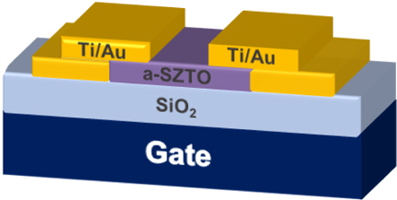
Heavily doped p-type silicon wafer was used as the substrate. Device fabrication started with a typical ultrasonic wafer cleaning process. A 0.5 M precursor solution of SZTO was prepared by the solution method, by dissolving a mixture of zinc acetate dehydrate [Zn (CH3COO)2·2H2O], tin chloride [SnCl2] and silicon tetraacetate [Si (OCOCH3)4] in 2-methoxyethanol [C3H8O2]. Monoethanolamine [C2H7NO] was then used as a solution stabilizer, and the mixture was stirred at 60℃. The mole ratio of Zn: Sn was fixed at 4:6, and silicon was added from 0.1 to 1. The solution was then stirred at room temperature for 12 h to form SZTO precursor. The precursor solution was filtered through a 0.2 μm syringe filter, and then spin-coated on silicon wafer at 3,000 rpm. The baking process was performed on a hot plate for 5 min under ambient air conditions, and annealing was carried out at 500℃ for 2 h under N2. Channel and electrode patterning was formed by photolithography and the wet etching process. The bottom-gate and top-electrodes were fabricated on SiO2 (200 nm)/heavily doped p-type Si wafer, where 70 nm electrodes of Ti/Au were deposited. The width and length of the active channel layer were 250 and 50 lm, respectively. The annealing process was performed at 500℃ for 2 h to improve the film quality.
Figure 1 shows a schematic of the SZTO TFT structure with the bottom gate and top contact electrode. Examination of the structural properties of SZTO thin films was carried out by X-ray diffraction (XRD). The electrical characteristics were measured with a semiconductor parameter analyzer.
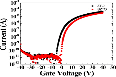
Figure 2 shows the electrical properties of SZTO TFT with increase of the Si ratio. The threshold voltage was shifted toward the positive direction, and the on-current was decreased with increasing Si content. In order to explain the effect of Si doping of solution processed TFTs, we applied the creation mechanism for the formation of different vacancies in the SZTO and ZTO. The oxygen vacancies in such systems are produced via dihydroxylation of M-OH and the alloy mechanism. Si has high binding energy with oxygen due to its low SEP. As a result, a decrease in the number of free electrons associated with decreased oxygen vacancy can be observed. In addition, the field effect mobility is decreased with increasing Si ratio from 0.1 to 1. The μFE was calculated using the following equation:
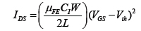
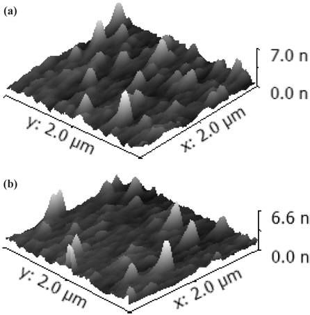
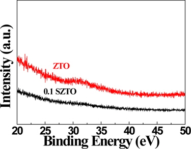
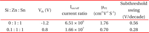
where Ci is the capacitance per unit area of the gate insulator, W and L are the channel width and length, and VGS and Vth are the gate bias and the threshold voltage, respectively. A summary of the TFT performance parameters according to the Si ratio is provided in Table 1, which includes the field effect mobility (μFE), threshold voltage (Vth), on-current (Ion), carrier concentration, and on-to-off current ratio (Ion/off). The ZTO TFT annealed at 500℃ displayed high performance, with the field effect mobility of 1.76 cm2/ V s and threshold voltage of −1.2 V, while the SZTO TFT annealed at 500℃ exhibited the field mobility of 0.7 cm2/ V s and threshold voltage of 0.8 V. Upon increase of the Si content, decreased μFE was observed in proceeding from ZTO to SZTO. As mentioned above, the oxygen vacancies in such systems are produced via dihydroxylation of M-OH and the alloy mechanism. The crystallinity of the SZTO films with different amounts of Si were next investigated via examination of the XRD patterns. As shown in Fig. 3, the broad peak revealed the solution processed SZTO films to be in the amorphous phase. No sharp peaks were observed in the XRD spectra. The amorphous phase of an active channel layer is an important point, because carrier transport in the channel layer of TFTs is considerably affected by the phase structure of the channel layer. The (n-1) d10ns0 electronic configuration of the metal elements in oxide semiconductors, such as ZnO, In-ZnO, and Si-In-ZnO, enables the formation of electron transport paths through the series of s orbitals [10]. Figure 4 shows the tapping-mode AFM images of 30-nm-thick ZTO and SZTO films on Si/SiO2 substrates. These films exhibited rms roughness values of 0.66 nm and 0.58 nm, respectively. The important transistor characteristic for TFT application is the device subthreshold swing.
Electrical characteristics of the ZTO and SZTO TFTs, including threshold voltage, on-to-off ratio, and μFE.

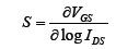
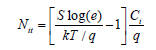
As in previous articles, the decrease in the subthreshold swing may be attributed to the interface and bulk trap density of the TFTs [11]. In general, charge trapping is characterized by the total trap density (Nt), including the bulk trap density (Nb) of the channel layer and the interface trap density (Nit) between the dielectric/channel. The decrease in the SS value can be attributed to the existing trap density in deep level states in the channel layer, including interface trap and bulk trap density. The addition of silicon atoms to the SZTO active layer causes the degeneration of oxygen vacancies since silicon can act as a carrier suppressor, consequently leading to a decrease in the on-current of the TFTs with increasing silicon content. The SS value also provides important information about the quality of a TFT. It is related to the Nit near the semiconductor/gate dielectric interface, by the equation:

where Ci, q, and k are the gate dielectrics capacitance per area, elementary charge, and the Boltzmann constant, respectively. In the case of SZTO channel TFTs, the trap site is observed near the conduction band edge, and is related to the doubly ionized oxygen vacancies [12-14]. The addition of silicon reduced the oxygen vacancy concentration in the SZTO channel. As a result, the Nit was considerably decreased, which contributed to improvement of the subthreshold swing characteristics. The Nt in the SZTO systems was decreased from 4.39 × 10¹² to 1.45×10¹¹ through its relation with the oxygen vacancy, which could be controlled by the addition of silicon to the SZTO system. Moreover, the SZTO TFTs are also suitable for fast switching devices due to their low S.S value of 0.28 V/decade.
In summary, SZTO thin film transistors were fabricated using the solution process. The incorporation of Si reduced the oxygen vacancies, acting as an oxygen binder. The Si acted as a carrier suppressor, allowing the SZTO TFT to achieve the following electrical properties: Vth = 0.8 V, μFE = 0.70 cm2 / V1 s1, S.S = 0.28 V/decade, and Ion/off = 1.66 × 10⁷. The annealing temperature of the solution processed oxide channel layer was high, at over 500℃. Moreover, with optimized semiconductor interfaces, the solution processed metal oxide device performance was enhanced to levels comparable to vacuum-deposited polysilicon or optimized metal oxide films.