Organic polymer dielectric thin films of styrene and vinyl acetate were prepared by the plasma polymerization deposition technique and applied for the fabrication of an organic thin film transistor device. The structural properties of the plasma polymerized thin films were characterized by Fourier-transform infrared spectroscopy, X-ray diffraction, atomic force microscopy, and contact angle measurement. Investigation of the electrical properties of the plasma polymerized thin films was carried out by capacitance-voltage and current-voltage measurements. The organic thin film transistor device with gate dielectric of the plasma polymerized thin film revealed a low operation voltage of −10V and a low threshold voltage of −3V. It was confirmed that plasma polymerized thin films of styrene and vinyl acetate could be applied to functional organic thin film transistor devices as the gate dielectric.
Organic thin film transistors (OTFTs) are representative organic electronic devices with flexible characteristic and low-cost process compatibility, and are often employed as sensors, display backplane, and rectifiers for radio frequency identification [1]. Recent research on OTFTs have been devoted to achieving low operation voltage to allow reduction of power consumption. High operation voltage is mainly caused by inferior permittivity/capacitance properties conferred by relatively thick polymer dielectrics, which could be solved by high-
The plasma polymerization technique is another alternative for the preparation of polymer dielectrics. Plasma polymerized polymers show excellent coating adhesion to any substrate, chemical/mechanical/thermal stability, high barrier effect, are pin-hole free and have flat surface structure formability. Most plasma polymers, which are distinguished from conventional polymers, consist of a structure that lies somewhere between the polymeric and inorganic materials, and is in the form of a highly cross-linked and highly branched three-dimensional network [2].
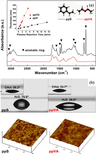
In the present study, a plasma polymerization method was proposed for application to a completely dry process for OTFT fabrication, which offers a one-step and a compatible process with the conventional process technologies. The OTFT devices had inverted staggered structure of Au/pentacene/plasma polymers/ITO. The effects of plasma polymerized polymer dielectric layers were studied for realization of low operation voltage of the OTFTs. Hydrophobic styrene and hydrophilic vinyl acetate [see Fig. 1(a) inset] monomers were used for the plasma polymerization of polymer dielectric layers.
ITO (150 nm, 12 Ω/cm2) coated glasses were used as substrates. The substrates were ultrasonically cleaned in acetone, ethanol, and distilled water, allowing removal of most of the organic contaminants on the ITO surface. Radio frequency (r.f.) capacitively-coupled plasma (CCP) was used for surface treatment of the ITO, with a system pressure of 0.1 Torr, Ar gas flow rate of 10 sccm, and main power of 100 W, carried out at room temperature. Without breaking the vacuum after plasma surface treatment, the plasma polymer layers were then deposited. Plasma polymerization of the styrene and vinyl acetate monomers was again done at room temperature using the CCP equipment. A detailed survey of the plasma polymerization processes can be found in various reviews and books, such as in references [2-5]. The plasma polymers were deposited under the following experimental conditions [see Fig. 1(a) inset]: main power of 200 W/bias power of 10 W, system pressure of 0.5 Torr, Ar gas flow rate of 30 sccm, and deposition time of 1-10 min through a shadow mask. The thickness was measured by evaluating micrographs of cross-sections of the plasma polymers using field emission-scanning microscopy (FE-SEM; Hitachi, S-430), and was found to be approximately 100 nm. A 70 nm-thick pentacene layer, as the active channel layer, and 100 nm-thick Au as the source/drain electrodes were then deposited using the thermal evaporation technique. The Au source/drain electrodes were patterned on the pentacene layer through a shadow mask.
Film composition, surface morphology, and electrical properties of the plasma polymers were investigated using Fourier transform infrared spectroscopy (FT-IR; Bruker Optics, Vertex 80 v) in a vacuum, contact angle measurement (Erma inc.), X-ray diffraction (XRD; Rigaku, M/Max 2,200 V/PC), atomic force microscopy (AFM; Digital instrument, Nanoscope Mutimode Ⅳ a) and a C-V analyzer (Keithley 590). To investigate the performance of the OTFTs, the current-voltage (I-V) characteristics were measured according to the applied voltage change using a source measurement unit (Keithley 2400) combined with another source measurement unit (Keithley 236).
Figure 1(a) shows the FT-IR spectra of the plasma polymerized styrene (ppS) and plasma polymerized vinyl acetate (ppVA) layers. The strongest absorptions of the ppS layer occurred for aromatic compounds in the region of 900~650 cm−1, due to C-H vibrations out of the plane of the aromatic ring. Most mono-nuclear and poly-nuclear aromatic compounds have peaks in the region of 3,080~3,010 cm−1, due to the stretching vibrations of the ring C-H bonds. Ring carbon-carbon stretching vibrations occur in the region of 1,625~1,430 cm−1. The formation of benzene rings in the ppS was likely due to non-destruction of the aromatic structure as a result of plasma bombardment. In the ppS and ppVA, the characteristic peaks for the conventional polymers, i.e. polystyrene and polyvinylacetate, showed comparatively weak and broader (but not absent) absorbance, suggesting significant amounts of fragmentation and rearrangement during the plasma deposition process. This may result in the formation of pinhole-free plasma polymer layers with highly cross-linked structure. Similar results were revealed by the FT-IR spectra of the plasma polymers, which identified chemical similarities and dissimilarities of the two materials as a result of a strongly system-dependent process. Figure 1(b) shows the contact angle measurements and AFM 3D-images of the plasma polymers. The surface energy of the ppS and ppVA layers was calculated from the contact angle measurements using distilled water (70.0° ±2% and 38.0° ±2%) and diiodomethane (29.2° ±2% and 33.7° ±2%) as the probe liquids. The geometric mean equation was used to calculate the surface energy [5]:
The surface energy of the ppS and ppVA layers was found to be approximately 45 and 64 mJ/m2, respectively. The lower surface energy of the ppS could be thought to be attributable to the higher density of the aromatic ring [6,7]. The AFM 3D-images of the 100 nm-thick layers of both ppS and ppVA grown on ITO are shown in Fig. 1(b). The root mean square (RMS) roughness of the ppS and ppVA layers was found to be approximately 0.296 and 0.265 nm, respectively. It could be seen that the plasma polymers had very flat surface structures with pin-hole free formability.
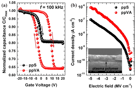
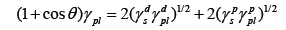
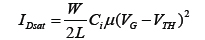
The capacitance of the gate dielectric, i.e. the thickness and dielectric constant, determine the operating voltage of the OTFTs [8-10]. The dielectric constants,
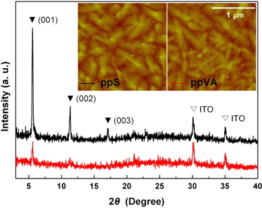
Figure 2 shows the x-ray diffraction (XRD) patterns and AFM image of the 70 nm-thick pentacene grown on the plasma polymer dielectrics. The XRD and AFM analyses were performed in order to investigate the effects of the surface properties of the plasma polymer dielectrics on the surface morphology of the pentacene. The corresponding XRD pattern contained a series of sharp (00
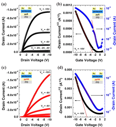
Figure 3(a) shows the
where
In summary, OTFT with plasma polymer dielectrics having high capacitive coupling could be operated at the low operation voltage of −10 V. The threshold and operating voltages were the lowest among those reported for polymer gate dielectrics. It was demonstrated herein that the plasma polymer dielectrics could be used in the fabrication of OTFT devices with favorable electrical properties, allowing significant improvement in the performance of the OTFT device. We believe that the proposed method provides an effective way to improve the electrical properties of plasma polymer dielectrics for OTFT devices, possibly by substituting the polymer dielectric through co-polymerization or double-layered structure.