A phase-locked loop (PLL) is implemented in frequency synthesizers that are used in many communication and digital systems [1,2]. For the circuit elements of PLL, it is important to consider the generation of a large number of precisely spaced frequencies that depends mostly on the frequency divider. Several techniques have been introduced to obtain a high-speed frequency divider [3-7], such as using a super-dynamic divider, multiplier, or injection-locked divider. A flip-flop circuit for use in broadband applications has a limitation in terms of speed because of the presence of a interconnection or gate-to-drain capacitance in MOS transistor. A dynamic circuit offers faster operation than a static circuit, and several techniques, including a super-dynamic circuit, have been proposed to improve the speed of the flip-flop. An injection-locked divider (ILFD) is an interesting implementation of a frequency divider because it can offer low power operation, and the conventional ILFD topology is similar to that of voltage controlled oscillator (VCO). A VCO that operates at high frequency of over 10 GHz requires an inductor which is usually rated at under a few tens of pico-Henries. Such low inductance is difficult to obtain in an integrated circuit (IC), furthermore, an integrated spiral inductor has an additional capacitance or resistance which prevent an improvement in the speed of the divider.
In this work, a current mode logic (CML) frequency divider with inductive peaking is used for analog PLL because it has a wide operating range with a high operating frequency and low power consumption.
The inductive peaking method was introduced in the 1940’s to enhance the bandwidth in an amplifier. An inductor was introduced with a load resistor to alter the frequency response of the amplifier, resulting in bandwidth enhancement by transforming the frequency response from a single pole to two poles.
Our work offers an inductive peaking and cascode circuitry in a CML frequency divider. Although inductive peaking is an old technique, the application of a cascode circuit can reduce the time-delay without degrading the bandwidth. With 0.18-μm CMOS process, 2:1 current-mode 20 GHz static frequency divider is presented. Its application to conventional PLL and its frequency synthesis are discussed with a post-layout CADENCE simulation.
2. CIRCUIT DESCRIPTION OF FREQUENCY DIVIDER
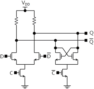
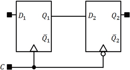
The purpose of frequency divider is to reduce the frequency of VCO output to that of the reference clock so that a proper comparison can be carried out. Static frequency divider with master-slave flip-flop operates over a wide range of frequencies, but it has a limitation with respect to the maximum operating frequency. Master-slave flip-flop is composed of D-latches which operate inversely to each other. Figure 1 is a CML D-lach with a differential pair and cross-coupled n-MOSFETs. Figure 2 is the master-slave flip-flop which is composed with the two D-latchs in Fig. 1. The master which is the first D-latch in Fig. 2 responds to D input before the slave. The master is positive-edge-triggered and the slave is negative-edge-triggered. If D = 1, the master sets on the positive clock transition. The high Q output of the master drives the next D input of the slave, so on an negative clock transition, the slave is set, repeating the action of the master. Compared to other flip-flops, the master-slave flip-flop has an advantage in that there are no-errors due to the time-delay of the clock pulse or the shapes of the pulse
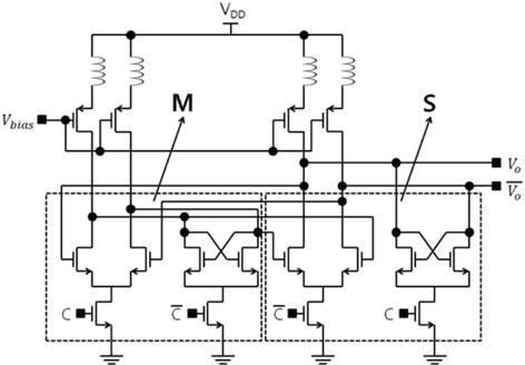
Conventional CML frequency divider [3], as seen in Fig. 3, is composed of two level-sensitive CML master-slave flip-flops. The divider achieves high division bandwidth to match the output of VCO. The master-slave flip-flops are switched by a pair of signals and use a resistor as a current source. The pair clock signals switch the current between the sample and hold operation of the flip-flops. The operation, as a divide-by-two circuit, can easily be verified by an analysis of a static operation of the master-slave flip-flops. The master-slave flip-flop acts as latch and read circuits. The read circuit is a differential pair in the block, and the latch circuit is of n-MOSFETs which are cross-coupled.
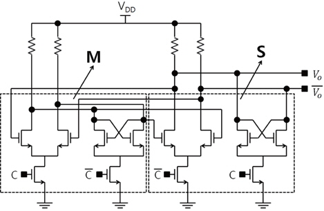
The proposed frequency divider is shown in Fig. 4, and the application of the cascode circuit [8] and the inductive peaking is shown for the proposed frequency divider. The resistor in the conventional CML frequency divider is replaced by a cascode circuit which is controlled by the DC bias gate voltage in the MOSFET. The cascode circuit in the integrated circuit (IC) can provide a superior frequency response and small resistance across the transistor. Since there is a small voltage drop across the transistor, the output swing is fully operational with a small supply voltage, and the time delay of the frequency divider can be significantly reduced by the cascode circuit.
Another application for the proposed frequency divider is that of inductive peaking [9,10] in the CML master-slave latches. Inductive peaking is known to increase the circuit bandwidth by trading the time delay. The inductor in series with a resistor delays the current flow at a high frequency, and the proposed inductive peaking with the cascode bias can increase the maximum frequency of the static divider with a wide enough frequency range to cover the VCO oscillation over 10-GHz.
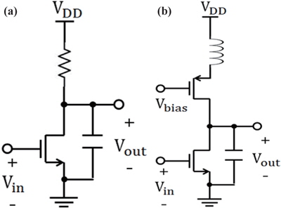
With respect to the common-source amplifiers Fig. 5(a) and (b), the basic circuit structure in the differential pair of the CML frequency divider is the common-source amplifier. The conventional and proposed CML dividers use the resistor and the cascode bias in the amplifier as a their respective current source. The proposed structure has a cascode circuit instead of a resistor, the cascode circuit has a high equivalent gain which provides the variable resistance and improve the frequency response. The equivalent resistance depends on the small signal parameters of the MOS transistor.
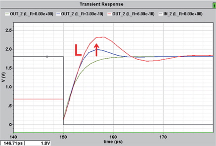
The inductive peaking structure extends the circuit’s band-width by inserting inductors that delay the current flows. The inductor in series with the load resistor causes the output voltage to have a sharp transition, and the inductive peaking is known to degrade the time delay by increasing the bandwidth. The switching characteristics of the amplifier with the inductive peaking structure are seen in Fig. 6, and it is measured at 10 MHz. The increase in the inductance L is associated with a longer on-off time-delay. Additionally, the peak voltage during the switching increases. In terms of the time-delay, the inductive peaking structure has no advantages in the CML frequency divider.
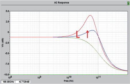
Figure 7 shows the simulated frequency response of the CML frequency divider with an inductive peaking structure. The result of the conventional divider which does not have an inductor is also included in Fig. 7. In the Bode magnitude plot, the 3 dB bandwidth increases from 20 GHz to 90 GHz with an increase in the inductance. The 20 GHz bandwidth is a result of when there was no inductance, and the result of Fig. 6 and Fig. 7 indicate that the inductive peaking structure increases the bandwidth although it provides a longer time delay as shown in Fig. 6. The bandwidth of the proposed frequency divider is increased more than 4 times over that of a conventional divider. The operating frequency and the power consumption can be limited mostly by the parameters of the MOS transistors in the frequency divider, and the parasitic capacitance in the MOS-FET and the metal-interconnect resistor should be minimized in order to obtain a high operating frequency with a low power consumption. The current driving capability of the frequency divider is also an important factor that can improve the operating frequency and can reduce the power consumption, which is the reason for the application of the cascode bias circuit in this work. In addition, the power consumption is in the trade-off with the frequency.
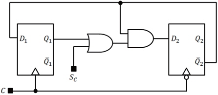
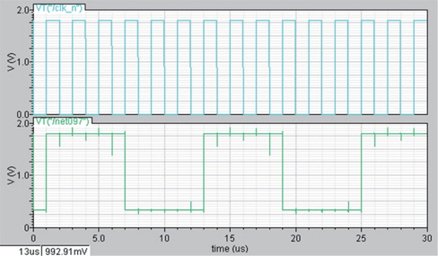
Figure 8 is the block diagram of the even and odd frequency divider, which is composed of the logic gates and D latches. The even (odd) clock frequency is obtained when the control signal Sc is high (low). Figure 9 is the outputs of the 6-divided signal which is a combination of the even (/2) and odd (/3) signals at an input frequency of 0.5 MHz and an input voltage of 1.8 V.
The proposed frequency divider is applied with five stages at an input frequency of 16.6 GHz. Figure 10 shows the result of the 32:1 divider which is the five stages of even divider. The simulation is performed by the CADENCE Spectre. The divide-by-32 of 16.6 GHz is about 0.5 GHz, and the expected output frequency of 0.5 GHz is obtained. The power consumption of the frequency divider is 6.9 mW at a load current of 3.85 mA.
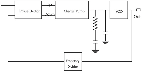
The proposed divider is applied in an analog PLL as a feedback circuit. The PLL in Fig. 11 consists of a phase detector (PD), charge pump (CP), low-pass filter (LPF), voltage controlled oscillator (VCO), and frequency divider. The integrated circuit (IC) of the PLL except the external LPF is designed with 0.18 μm CMOS process with 3.3 V supply.
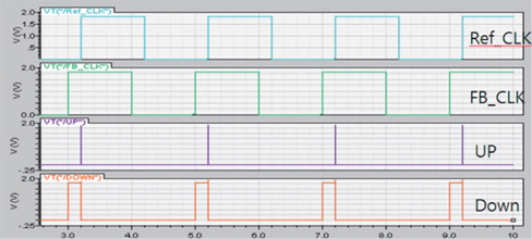
In Fig. 12, the output of the phase detector shows the pulses at the UP and DOWN nodes. The pulse at the UP node shows to be driven by the rising edges of the reference clock (Ref_CLK), while the pulse at the DOWN node is driven by the rising edges of the feedback signals (FB_CLK). The signal FB_CLK is the output of the frequency divider. In a phase detector (PD), the falling edges of the reference clock that comes at the end of period time influence the width of pulse at the UP signal since the transition from a low to a high logic at UP is controlled by the reference clock.
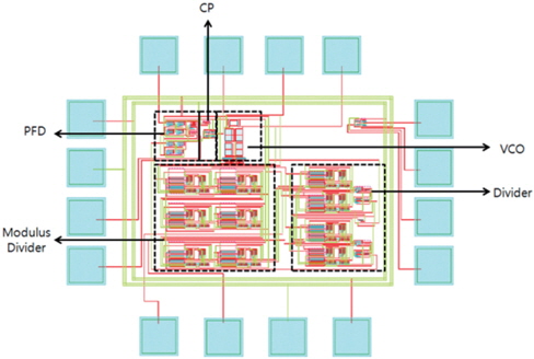
Figure 13 shows the chip layout photo of the PLL, as shown in Fig. 11. The area of the circuit including the PADs is approximately 0.3 mm2. The inductor inside the frequency divider and the capacitor from low-pass filter (LPF) are designed off-chip, and in the proposed frequency divider, an off-chip inductor of 0.3 nH is connected to the divider.
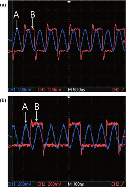
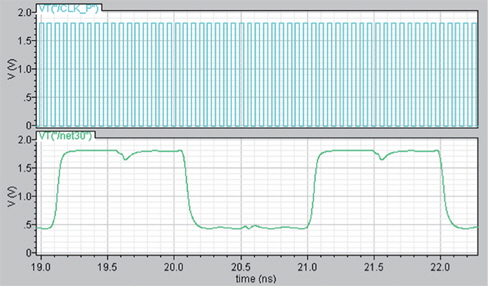
The experimental clock signals in the oscilloscope are shown in Fig. 14, where Fig. 14(a) shows the input signal A of 20 MHz and the output signal B of 10 MHz which is an even clock pulse. Fig. 14(b) shows the odd clock pulse B of 10 MHz at an input frequency of 30 MHz. The even and odd frequencies are obtained as expected. The result therefore indicates that the proposed CML frequency divider operates properly as a feedback circuit in an integrated PLL.
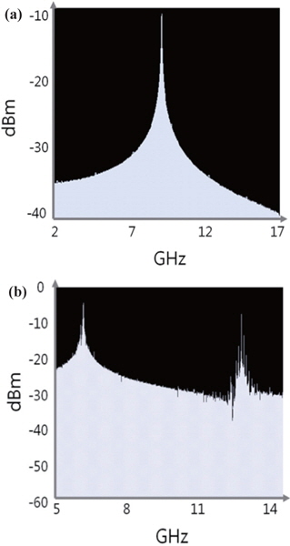
Figure 15 shows the frequency spectrum of CML frequency divider with and without inductive peaking. It is obtained at the input frequency of 20 GHz with a power consumption of 2 dBm. Fig. 15(a) and (b) are the result of a frequency divider with and without an inductive peaking technique, respectively. Fig. 15(a) shows that the divide-by-two operation indicates a peak at 10 GHz which is the same signal of 20-GHz / 2, on the other hand, Fig. 15(b) shows an inaccurate operation. Performance summary of the proposed divider is shown in Table 1.
[Table 1.] Performance summary.
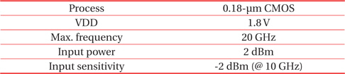
Performance summary.
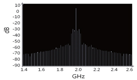
The proposed divider is applied in PLL and tested with a divide-by-eight circuit which uses three dividers. Fig. 16 is the output frequency spectrum of the PLL with an input frequency of 250 MHz. The output frequency spectrum is obtained by using a divide-by-eight circuit. Fig. 16 shows the peak at 2 GHz, which is indicated by the 250 MHz X 8 signal. The reference spur is about -64 dBc and the power consumption is 13 mW. This indicates that the proposed CML divider operates properly with low power consumption. The input sensitivity, which is the required input power, is obtained to be -2 dBm at a divider frequency of 10 GHz. A comparison with other works is provided in Table 2.
[Table 2.] Comparison of the performance.
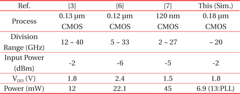
Comparison of the performance.
This paper describes a high frequency CML frequency divider which includes an inductive peaking circuit with a cascode bias. The CML frequency divider includes two D-latches which works as a master-slave flip-flop. The master-slave flip-flop is composed of a differential pair, cross-coupled latch, and current-sources. The cascode bias in the inductive peaking circuit is designed to provide a high current driving capability and a stable frequency response. The even/odd and the multiples of the divide-by-two operation are obtained. CML frequency divider is integrated in 0.18-μm CMOS process, and a post-layout simulation shows that the proposed divider operates at 20 GHz with a low power consumption of 6.9 mW. The frequency divider is applied in PLL system as a feedback circuit, where the divide-by-eight circuit operates at 2 GHz input frequency with power consumption of 13 mW. Compared to a conventional frequency divider, the proposed divider shows an increase in the band-width, although the switching characteristic shows a longer time-delay with an inductive peaking structure.