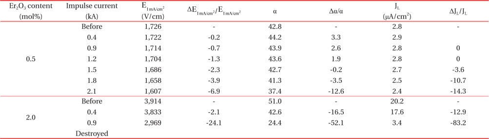
In light of the sure protection function, the most important factors of a varistor are the clamping voltage ratio and degradation characteristics. The degradation characteristics of Pr/Co/Cr/Er co-doped zinc oxide varistors were investigated by impulse currents (0.4~2.1 kA) stress for the specified content of Er2O3 (0.5 and 2.0 mol%). The varistor doped with 2.0 mol% Er2O3 exhibited the best clamp characteristics, with the clamp voltage ratio (K) in the range of K = 1.63~1.88 at the impulse currents of 5-50 A. However, the varistor doped with 0.5 mol% exhibited excellent electrical stability, with variation rates for the breakdown field, for the nonlinear coefficient, and for the leakage current density of −6.9%, −12.6%, and −14.3%, respectively, after application of an impulse current of 2.1 kA. In contrast, the varistor doped with 2.0 mol% was destroyed after application of an impulse current of 1.2 kA.
Zinc oxide varistors are polycrystalline electroceramic devices formed by sintering zinc oxide with primary and/or subordinate additives such as bismuth, praseodymium, cobalt, manganese, chromium, antimony, etc [1]. They are voltage clamping or voltage switching devices which act with the level of voltage in which impedance decreases abruptly when the voltage is increased up to threshold voltage, called the varistor voltage. They clamp overvoltage to the varistor voltage when voltage exceeds the threshold value. At low voltages, they act as high value resistors such as insulators, obeying ohm’s law. They possess excellent surge-withstanding capability because zinc oxide varistors are multi-junction devices, consisting of the microstructure of semiconducting ZnO grain (S)-insulating intergranular layer (I)-semiconducting ZnO grain (S) (unit structure of SIS type), unlike the Zener diode of a single junction [2]. Zinc oxide varistors have been used extensively in the field of circuit overvoltage protection, with applications ranging from a few volts in electronic circuits to millions of volts in electric power systems [3,4].
Most investigations on Zn-Pr6O11-based varistors have reported about the microstructure and electrical properties in terms of additives and the sintering process [5-18]. In particular, Nahm et al. reported the effect of rare earth oxides on the electrical properties and the resulting stability against DC accelerated degradation stress [8-11,13].
In application of varistors, the nonlinearity and its stability, as well as the surge withstanding capability are important factors, which need consideration. Protection of electronic equipment and electrical power systems from various surges demands varistors with high stability in order to enhance reliability. Therefore, the electrical stability against surge stress is technologically very important in zinc oxide varistors [13]. However, studies on the degradation characteristics of ZnO-Pr6O11- based varistors against high energy surges have rarely been reported [17,18]. In this work, the degradation characteristics of Pr/Co/Cr/Er co-doped zinc oxide varistors [10] were investigated for the specified content of Er2O3 by application of impulse current stress.
The composition of the varistor samples was as follows: (98.0-x) mol% ZnO, 0.5 mol% Pr6O11, 1.0 mol% CoO, 0.5 mol% Cr2O3, and x mol% Er2O3 (x = 0.5 and 2.0, all reagent-grade). Raw materials were blended by ball milling with zirconia balls and acetone as the dispersion medium in a polypropylene bottle for 24 h. Each blend was dried at 120℃ for 12 h and then calcined in air at 750℃ for 2 h. The calcined blends were pulverized using an agate mortar/pestle, after which the 2 wt% polyvinyl alcohol (PVA) binder was added, granulated by sieving through a 100-mesh screen to produce the starting powder. The powder was pressed into disk-shaped pellets of 10 mm diameter and 2 mm thickness at a pressure of 80 MPa. The pellets were sintered at 1,340℃ for 2 h and furnace-cooled to room temperature. The heating and cooling rates were 4℃/min. The sintered pellets were lapped and polished to 1.0 mm thickness. The final pellets were about 8 mm diameter and 1.0 mm thickness. Silver paste was painted on both faces of the pellets, and the electrodes were formed by heating at 600℃ for 10 min. The electrodes were 5 mm in diameter. Finally, lead wire was soldered on both electrodes, and the samples were packaged by dipping them into a thermoplastic resin powder.
2.2 Microstructure examination
For characterization of the microstructure, either side of the samples were lapped and ground with SiC paper, and then polished with 0.3 μm-Al powder to a mirror-like surface. The polished samples were thermally etched at 1,100℃ for 30 min. The surface microstructure was then examined by a scanning electron microscope (SEM, Hitachi S2400, Japan). The average grain size (d) was determined through the lineal intercept method using the expression d = 1.56 L/MN, where L is the random line length on the micrograph, M is the magnification of the micrograph, and N is the number of grain boundaries intercepted by the lines [19]. The density (ρ) of the sintered pellets was measured using a density determination kit (238490) attached to a balance (Mettler Toledo AG 245, Switzerland).
The electric field-current density (E-J) characteristics were measured using a V-I source (Keithley 237). The breakdown field (E1mA/cm2) was measured at 1.0 mA/cm2, and the leakage current density ( JL) was measured at 0.8 E1mA/cm2 . The nonlinear coefficient (α) was defined by the empirical law, J = C·Eα, where J is the current density, E is the applied electric field, and C is a constant. α was determined in the current density range of 1.0 mA/cm2 to 10 mA/cm2, where α = 1/(logE2-logE1), and E1 and E2 are the electric fields corresponding to 1.0 mA/cm2 and 10 mA/cm2, respectively.
2.4 Clamping voltage measurement
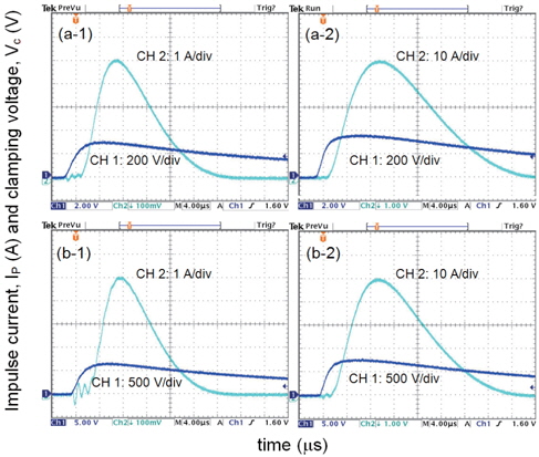
The clamping voltage (Vc) was measured at impulse currents (Ip) of 5, 10, 25, and 50 A using a surge generator (Tae-yang Engineering, Busan, Korea) and an oscilloscope (TeK3020B, Beaverton, Oregon, USA). The Ip waveform had a width of 20 μs and a rise time of 8 μs (8×20 μs). The clamp voltage ratio (K = Vc/V1mA ) was determined from the ratio of Vc to the breakdown voltage measured at the current of 1.0 mA DC (V1mA).
The impulse degradation test was performed on a surge generator at multi-impulse currents of 0.4, 0.9, 1.2, 1.5, 1.8, and 2.1 kA (three times continuously for each Ip). Ip had a width of 20 μs and a rise time of 8 μs (8×20 μs). An interval of 10min was provided between different Ip cycles for the same sample. After application of the respective multi-impulse current, the V-I data were measured at room temperature.
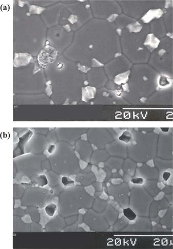
SEM micrographs of the samples are shown in Fig. 1. The samples had a simple microstructure consisting of a Pr-rich and Er-rich layer as a minor secondary phase (whitish area), in addition to the primary phase of ZnO bulk [10]. Increasing content of Er2O3 generated higher amounts of secondary phase, which existed mainly at the grain boundary and nodal point. The average grain sizes (d) were 12.1 and 6.8 μm, respectively, for the specified content of Er2O3 (0.5 and 2.0 mol%). The densities (ρ) of the sintered pellets for the samples were 5.54 and 5.35 g/cm3 (theoretical density 5.78 g/cm3 in ZnO), respectively [10].
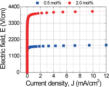
Figure 2 shows the E-J characteristics of the samples with the specified Er2O3 content (0.5 and 2.0 mol%). It can be seen that the conduction characteristics were composed of a linear region with OFF state for flowing current before the breakdown field and a nonlinear region with ON state for flowing current after the breakdown field. The E-J characteristic parameters calculated from Fig. 2 are listed as initial values in Table 2. The breakdown field ( E1mA/cm2 ) increased significantly from 1,726 to 3,914 V/cm for the specified Er2O3 content (0.5 and 2.0 mol%). This was attributed to the increase in the number of grain boundaries caused by the decrease in the average ZnO grain size, for constant thickness (1 mm) of the sample. On the other hand, the nonlinear coefficient (α) increased from 42.8 to 51.0 for the specified Er2O3 content (0.5 and 2.0 mol%). The increase of the α value may be attributed to the increase of the Schottky barrier height because of the increase of the interface state density at the grain boundaries with increasing Er2O3 content.

E-J characteristic parameters of the samples before and after application of an impulse current.
The clamping voltage (Vc) corresponding to the impulse currents of 5 and 50 A applied to the samples with specified Er2O3 content (0.5 and 2.0 mol%) is shown in Fig. 3. Clamping voltage (Vc) is an important feature of a transient suppressor. Because all protective devices are connected in parallel with the device or system to be protected, a lower clamping voltage will apply less stress to the protected devices. Strictly speaking, the magnitude of the clamping voltage (Vc) does not determine the performance of the varistors. This is selected in light of the insulation strength of the system connected in parallel with the varistors. Really what is more important is the clamp voltage ratio (K) as a figure of merit in the varistors. The clamp voltage ratio (K) decides how much the nonlinearity is maintained until the high current region. The lower the clamp voltage ratio (K), the better the camping characteristics. The clamping voltage (Vc) is defined by the drop voltage between electrodes of the sample when the specified impulse current flows through the sample [18,19]. For the sample doped with 0.5 mol% Er2O3, the clamping voltage (Vc) increased from 304 V to 360 V when the impulse current increased from 5 A to 50 A. Then, the clamp voltage ratio (K) increased in the range of K = 1.7~2.01. On the other hand, the clamping voltage (Vc) of the sample doped with 2.0 mol% Er2O3 increased from 660 V to 760 V when the impulse current increased from 5 A to 50 A. Then, the clamp voltage ratio (K) increased in the range of K = 1.63~1.88. Therefore, the sample doped with 2.0 mol% Er2O3 exhibited a lower clamp voltage ratio (K) than the sample doped with 0.5 mol% Er2O3. This resulted from the difference of the nonlinear coefficient (α). In general, higher values of the nonlinear coefficient (α) will lead to lower K values. For example, the nonohmic coefficient in the high current region was calculated through the expression, α = (logIp2−logIp1)/(logVc2−logVc1), where Ip1 = 5.0 A, Ip2 = 50 A, and Vc1 and Vc2 are the clamping voltages corresponding to Ip1 and Ip2, respectively. The samples doped with Er2O3 exhibited nonlinear coefficients of 13.6 and 16.3, respectively, for the specified Er2O3 content (0.5 and 2.0 mol%). The clamping voltages (Vc) and clamp voltage ratios (K) corresponding to the lower impulse currents of 5~50 A for the samples are summarized in Table 1.

Clamping voltage (Vc) and clamp voltage ratio (K) of the samples corresponding to different impulse currents.
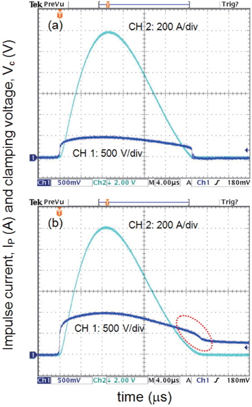
Figure 4 shows the impulse current waveform of 1.2 kA in order to investigate the degradation characteristics against higher impulse currents of 0.4~2.1 kA applied to the samples. It seems that the sample doped with 2.0 mol% Er2O3 was destroyed after application of an impulse current of 1.2 kA in light of the wave tail in the clamping voltage (Vc) waveform. The point at which the wave tail was no longer sharp may be indicative of destruction.
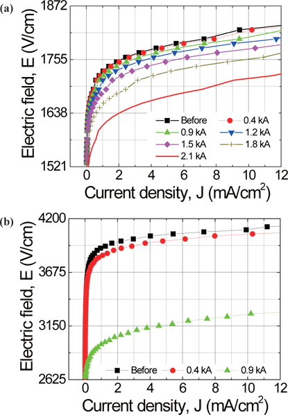
The variation of E-J characteristics after application of higher impulse currents of 0.4-2.1 kA are compared with the initial E-J characteristics of the samples in Fig. 5. It can be seen that the E-J characteristic curves shifted toward a low field region (downward in Fig. 5) in the breakdown region after application of the impulse current. This is entirely different with the E-J characteristic behavior, which shifted toward a high current region (rightward) in the pre-breakdown region after application the DC accelerated degradation stress [11]. The sample doped with 0.5 mol% Er2O3 exhibited the smallest variation of the E-J characteristics in the nonlinear region over the test impulse current. In contrast, the sample doped with 2.0 mol% Er2O3 exhibited a large variation in the nonlinear region after application of an impulse current of 0.9 kA. This sample was destroyed at an impulse current of 1.2 kA, and exhibited ohmic characteristics. The sample doped with 2.0 mol% Er2O3 possessed many pores and a higher amount of secondary phase at the grain boundary and triple point. This resulted in decrease of the effective area of the grain boundary [11]. Therefore, the failure against the impulse current can be attributed to very high impulse current density per grain boundary due to the many pores and high amount of secondary phases.
The variations of the breakdown field (ΔE1mA/cm2/E1mA/cm2), of the nonlinear coefficient (Δα/α), and of the leakage current (ΔJL/JL) after application of impulse currents to the samples are summarized in Table 2. ΔE1mA/cm2/E1mA/cm2 after application of an impulse current of 0.9 kA was -0.7% for the sample doped with 0.5 mol% Er2O3 and -24.1% for the sample doped with 2.0 mol% Er2O3. After application of an impulse current of 2.1 kA, the value of -6.9% was obtained for the sample doped with 0.5 mol% Er2O3, whereas the sample doped with 2.0 mol% Er2O3 exhibited a short-circuit. The sample doped with 0.5 mol% Er2O3 showed very good stable breakdown field (E1mA/cm2) characteristics against the impulse current, recording a variation rate much less than the 10% specification for commercial varistors. After application of an impulse current of 0.9 kA, Δα/α was −2.6% for the sample doped with 0.5 mol% Er2O3 and −52.1% for the sample doped with 2.0 mol% Er2O3. Furthermore, Δα/α for the sample doped with 0.5 mol% Er2O3 was only −12.6% after application of an impulse current of 2.1 kA. On the other hand, the leakage current density (JL) for the sample doped with 0.5 mol% Er2O3 did not vary after application of an impulse current of 1.2 kA. Therefore, it was clear that the sample doped with 0.5 mol% Er2O3 possessed much higher surge-withstanding capability than the sample doped with 2.0 mol% Er2O3. As a result, it can be seen that the Er2O3 content had a significant effect on the stability against impulse current stress. In other words, it was confirmed that the secondary phases located at the nodal point and intergranular layer, as well as the pores, had a severe effect on the impulse degradation characteristics.
The degradation characteristics of Pr/Co/Cr/Er co-doped zinc oxide varistors were investigated by subjecting the samples to impulse current stress (0.4~2.1 kA). The sample doped with 2.0 mol% Er2O3 exhibited a lower clamp voltage ratio (K) under impulse currents than that doped with 0.5 mol% Er2O3. The clamp voltage ratio (K) of the varistor doped with 2.0 mol% Er2O3 was in the range of K = 1.63~1.88 at the impulse currents of 5~50 A. However, the best electrical stability against the impulse currents of 0.4-2.1 kA was obtained by the varistor doped with 0.5 mol% Er2O3, which exhibited ΔE1mA/cm2 / E1mA/cm2 = −6.9%, Δα/α = −12.6%, and ΔJL/JL = −14.3% after application of an impulse current of 2.1 kA. In conclusion, Pr/Co/Cr/Er co-doped zinc oxide made under this sintering condition is capable of being applied in surge protection devices (SPD).