Since the first demonstration of functional metal-oxide-semiconductor field-effect transistors (MOSFETs) with high-k gate dielectrics, the interest in germanium (Ge) has increased significantly [1]. In addition, Ge has gained significant attention as an alternative channel material for high-speed complementary metal-oxide-semiconductor (CMOS) devices due to its higher electron and hole mobilities compared to Si [2]. Metal/Ge contacts offer the potential to study fundamental properties of interfaces, and metal source/drain (S/D) is considered as a good approach to dopant activation in n-Ge [3]. The metal S/D junction is also required to reduce parasitic resistances of ultra-scaled CMOS devices. However, the low-solubility of n-type dopants in Ge causes incomplete activation [4]. Moreover, strong Fermilevel pinning (FLP) at the charge neutrality level (CNL) close to the valence band edge EV of Ge has resulted in a high Schottky barrier height (SBH) at the metal/n-Ge interface [5], which has acted as a significant challenge in obtaining low barrier height metal contacts to n-Ge and has hampered the development of Ge-based devices. The lack of low resistance S/D contacts in the Ge n-MOSFETs limits the maximum current. Hence, many research reports have focused on alleviating the FLP; i.e., the Fermi level of the metal is released toward the conduction band of Ge, yielding a lower SBH.
As a widely used method to reduce the SBH in n-Ge, the introduction of a thin insulating layer, such as TiO2 [6], Al2O3 [7], MgO [8], and GeOx [9] between the metal and Ge, has been researched as a tunneling barrier. As a possible mechanism, the inserted insulating layer could block the electron wave function from metal to semiconductor, which eventually reduces the density of metal induced gap states (MIGS) [5]. It has also been suggested that the dipole formed at the metal/semiconductor (MS) interface would cause the potential drop, modulating the SBH [10]. Using the structure of the metal/TiO2/n-Ge contact, it has been suggested that the main cause of the reduced SBH is not the release of the FLP effect but the shift in the pinning position [11].
Due to the technical importance of metal-semiconductor (MS) contacts, understanding the nature of the defects present in semiconductors and the relevant current transport across the MS contacts is essential. One of the important factors for the Schottky junction is to understand the process that determines the flow of electrons over the Schottky barrier when a bias voltage is applied to the junction. Analysis of the electrical characteristics of the Schottky diodes at room temperature is useful. However, it does not provide detailed information about the conduction process, the nature of barrier formed at the interface and the interface states.
These interface states can play an important role in the current transport property and carrier recombination processes during device operation. The temperature-dependent electrical characteristics allow us to understand the conduction mechanisms more thoroughly and evaluate the validity of the thermionic emission theory. In addition, the change in surrounding temperature affects the main diode parameters, such as SBH, ideality factor and series resistance. Therefore, it is crucial to analyze the electrical properties at the MS interface in a wide temperature range. The temperature dependence of current-voltage (I-V) characteristics allows us to understand the different aspects involved in the current transport mechanism. However, most previous studies on Schottky contacts to n-Ge have been limited to the electrical characterization at room temperature and there is little knowledge regarding current transport characteristics in n-Ge Schottky diodes at low temperatures [12,13].
In this research, we investigated the temperature-dependent forward bias electrical properties in Cu/n-type Ge Schottky contacts in the temperature range of 100~300 K and an analysis was performed to extract information about the current transport mechanism.
In this investigation, single side polished n-type Ge (100) (Sb-doped) wafers (thickness: 500 μm), grown by the Czochralski method, were used as the starting material. The roomtemperature carrier concentration was about ~1 × 1016 cm-3. Before Schottky contact formation, oxygen plasma treatment was performed on the polished side to remove the native oxide layer. Oxygen plasma was produced with a plasma power of 100 W, an atmospheric pressure, and an oxygen flow rate of 40 sccm and an Ar flow rate of 8 sccm. Copper (Cu) Schottky contacts with a thickness of 100 nm were deposited by radio-frequency (RF) magnetron sputtering through a shadow mask onto the polished side after cleaning it with solvent. For the Ohmic contact, Al metal with a thickness of 150 nm was deposited over the entire back surface of the samples. Here, we did not perform thermal annealing to improve the ohmic contact characteristic because we wanted to prevent any chemical reaction from thermal annealing at the Cu/n-Ge interface. Temperature-dependent current-voltage (I-V) measurements were performed with a HP 4156B semiconductor parameter analyzer and a cryogenic probe station (Janis ST-500).
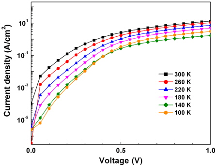
Figure 1(a) shows the semi-logarithmic forward bias I-V characteristics measured over a temperature range of 100~300 K. The diode revealed the rectifying characteristics at all measured temperatures. The forward bias I-V characteristics of a Schottky diode are given by the following equations using the thermionic emission (TE) model [14].


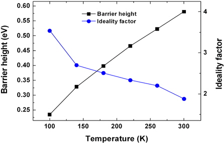
where I0 is the reverse bias saturation current, A is the contact area, A** is the effective Richardson constant (140 Acm-2K-2 for n-type Ge), ΦB is the SBH at zero-bias, n is the ideality factor, V is the applied bias voltage, and RS is the series resistance. For values of V greater than 3 kT/q, the ideality factor can be obtained from the slope of the linear region of the ln(I)-V curves. Here, both the ideality factor and SBH were extracted from the forward bias region from 0.1 to 0.2 V. The temperature dependence of the ideality factor and the barrier height determined from I-V measurements are shown in Fig. 2. It can be seen that both parameters exhibit strong temperature dependence. For example, the ideality factor decreases from 3.54 to 1.88 and the barrier height increases from 0.23 to 0.58 eV as the temperature increases from 100 to 300 K. Since both the SBH and ideality factor are constant with temperature in the TE model, such temperature dependence implies the deviation from the pure TE model. This anomalous behavior of both the SBH and ideality factor is commonly observed in real Schottky contacts and could be associated with the spatially inhomogeneous Schottky barrier [15]. Using a highresolution transmission electron microscope (HR-TEM), Janardhanam et al. showed the presence of a nonuniform interfacial layer in the Se/Ge interface, which resulted from an interfacial reaction between Se and Ge occurring during Se deposition [12]. Such a nonuniform interfacial layer was attributed to a combination of low and high barrier patches at the interface, responsible for spatially inhomogeneous Schottky barrier. Likewise, the presence of a nonuniform interfacial layer between Cu and n-Ge in this research might produce an inhomogeneous Schottky barrier. Since current transport at the metal-semiconductor (MS) interface is a temperature activated process, electrons at low temperatures can surmount the lower barriers and, therefore, current transport will be dominated by current flowing through the patches of small regions with a lower SBH and a larger ideality factor [16,17]. By increasing the temperature, more electrons have sufficient energy to surmount the higher Schottky barrier. As a result, the dominant barrier height will increase with the temperature. The relatively large ideality factor has been attributed to the presence of barrier height inhomogeneity at the interface, the presence of a thin interfacial native oxide layer and formation of interfacial states [16,17].
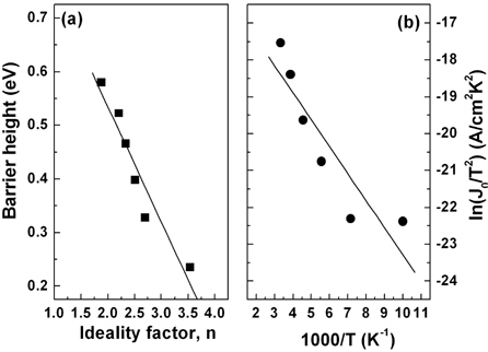
Figure 3(a) shows the plot of SBH values as a function of the ideality factor. There is a linear relationship between the SBH and the ideality factor and the lateral inhomogeneity in the Schottky barrier explains this linear relationship[17]. A homogeneous SBH of 0.73 eV was obtained from the plot of SBH vs. the ideality factor by extrapolating to n = 1. An activation energy plot was also considered to determine the SBH and the Richardson constant. Using Eq. (2), the conventional Richardson plot can be written as:

Using the values of the saturation current density J0 at each temperature from the current density-voltage (J-V) data shown in Fig. 1, the conventional Richardson plot of ln(J0/T2 ) versus 1,000/T was obtained in the temperature range of 100~300 K. From the linear fit to the plot in Fig. 3(b), the SBH and Richardson constant were found to be 0.06 eV and 1.17 × 10⁻⁷ Acm-2K-2, respectively. The SBH obtained from the conventional Richardson plot is much smaller than those from the I-V method. From Fig. 3(b), we can see that the data points, except the point at 100 K, fit well on a straight line. The nonlinearity at low temperatures was due to the temperature dependencies of the SBH and the ideality factor. In particular, the Richardson constant is much lower than the theoretical value of n-Ge (140.0 Acm-2K-2). Such a large discrepancy between the experimental and the theoretical values of the Richardson constant may be due to the spatial fluctuation of the barrier height in our contacts [18].
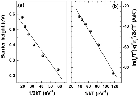
In order to explain the observed barrier inhomogeneity, we employed a Gaussian distribution of SBH over the contact area characterized by a zero-bias mean barrier height and a standard deviation (σ0), given by [15]:

As shown in Fig. 4(a), the linear fit to the plot of φB versus 1/2 kT produced the values of and σ0 =0.092 V. It is evident that the value of σ0 is not small compared with the mean SBH value and it indicates the inhomogeneity of the barrier at the MS interface. Thus, we adopted the modified Richardson plot, taking into account barrier inhomogeneity. The modified Richardson plot is give by [15]:

From the plot in Fig. 4(b), the SBH and the Richardson constant were calculated to be 0.72 eV and 392.5 Acm-2K-2. The obtained Richardson constant is higher than the theoretical value of n-Ge. However, this value is much closer to the theoretical value compared to the value from the conventional Richardson plot. Using the modified Richardson plot in the temperature range of 140~300 K, Chawanda et al. obtained the Richardson constant of 1.37 Acm-2K-2 for the Se/n-Ge Schottky contact [13]. They attributed the discrepancy between the theoretical and the obtained Richardson constants to a large degree of inhomogeneity at the interface. A similar explanation can be applied to the Cu/n-Ge Schottky junction in this work.
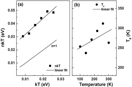
The temperature dependence of the ideality factor in Schottky contacts, called a T0 effect, takes the form of n(T)=1+T0/T, where T0 is a constant which is independent of temperature and voltage over a wide temperature range [19,20]. The plot of nkT versus kT should appear as a straight line with a slope equal to unity, and an intercept giving the T0 value. Fig. 5(a) shows the values of nkT as a function of kT. For ideal Schottky diodes, the T0 value approaches zero with the ideality factor equal to one. The linear fit to the plot in Fig. 5(a) produced a straight line with a slope of 1.21, which is not parallel to that of the ideal Schottky diode (n=1). As shown in Fig. 5(b), when the T0 values determined by using the temperature dependent n values are described as a function of temperature (i.e., using the form of T0=(n-1)T), T0 can take form as follows [20]:

The values of and α are found to be 230.0 K and 0.21, from the intercept and slope of the straight line fitted to the experimental data, respectively. Such strong temperature dependence of T0 values are associated with the strong temperature dependence of both the SBH and ideality factor and suggest a large degree of barrier inhomogeneity or the contribution of recombination and tunneling current components [20,21].
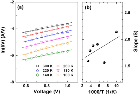
In the case of the uniform distribution of localized defect states, the current values can be described in the frame of space charge limited current (SCLC) transport theory, expressed as [22]:

where n0 is the density of the thermally-activated carriers, μ is the mobility and d is the electrode spacing. According to Eq. (7), the S parameter can be obtained from the slope of the ln(I/V) vs. V plot, which is defined as [22]:

where Nt is the density of the localized states near the Fermi level. The plots of ln(I/V) vs. V at different temperatures for a high forward bias region are plotted in Fig. 6(a). As seen from the figure, the curves show linearity for all the temperatures and the S values were obtained from the slopes of these curves. The variation of S slopes with the inverse of temperature is shown in Fig. 6(b). The decrease in the S values with increasing temperature is observed; this decrease is is in accordance with the SCLC transport theory. The carriers trapped at the localized defect states can be thermally excited to the conduction band with increasing temperature. Hence, the current transport in the high electric conduction region is controlled by the injected space charge [23]. From the slope of S vs. 1,000/T plot shown in Fig. 6(b), the Nt value was determined to be 1.46 × 10¹² eV-1 cm-3.
We investigated the temperature dependent electrical properties of Cu Schottky contacts to n-type Ge in the temperature range of 100~300 K. The barrier height increased and the ideality factor decreased with increasing temperature. Spatially inhomogeneous Schottky barriers distributed over the contact area could be the main cause of such temperature dependence of the barrier height and the ideality factor. A notable deviation of the Richardson constant from the theoretical value was observed, and this also assured the inhomogeneity of the barrier. The density of localized defect states (Nt) obtained by applying the theory of SCLC transport; the density was obtained as 1.46 × 10¹² eV-1 cm-3.