For several years, polymer materials have been employed as an insulator for high-voltage devices and other equipment because of their excellent electrical properties, such as high breakdown stress and low conductivity [1]. When DC voltage is applied to a polymer insulator, a space charge is formed in the bulk. Generally, the presence of space charges in insulating materials distorts the electric field distribution, leading to a local electric field enhancement within the insulating material that can cause insulation degradation and ultimately electrical breakdown [2].
In fact, space charge behavior in insulating polymers such as XLPE and LDPE is not yet well understood.
There are two main difficulties concerning this: firstly, the space charge in insulating polymers depends on many factors, such as the morphology of the insulation, conductivity, permittivity, roughness interface, electrode material, applied electric field, and temperature.
Secondly, measuring space charge distribution in a dielectric material is very difficult. There has been recent progress in space charge measurement techniques, such as the pulsed electroacoustic (PEA)[1,2,7] method and the induced pressure pulse (LIPP); however, measurement still remains difficult since the PEA and LIPP systems only give a net charge density, and the shape of the capacitive charge at the two electrode-interfaces is always different.
For several years, the theoretical modeling and simulation have been integrated for better understanding of the space charge dynamics [3-8]. Many previous works showed the existence of two charge dynamics corresponding to mobile and trapped carriers at high DC voltages applied, respectively .
Among the important parameters in studying the space charge dynamics in insulators are the transient and steady state currents. Their evolution can determine the conduction mechanism in the insulators under the applied voltage. According to our knowledge, few numerical works have been presented, especially for the transient current of the bipolar charge transport in the insulating polyethylene.
The main objective of the present study is to provide a better understanding of the mechanisms responsible for the formation and the generation of the space charge packets. For that purpose, we have investigated the symmetrical model that confirms the existence of two dynamics of charges which depend on the applied voltage.
2. DESCRIPTION OF THE PHYSICAL MODEL
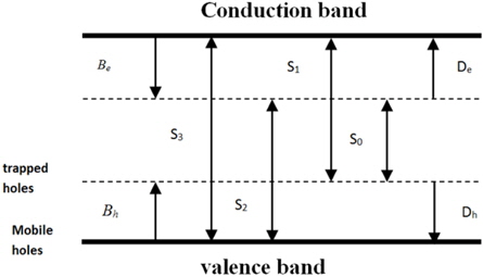
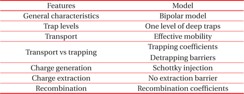
In our model, we consider a 150-μm thickness polyethylene film sandwiched between two electrodes under DC applied voltage. The contact electrode polyethylene is supposed to be perfect. The model is one-dimensional, symmetrical, the described bipolar charge transport in low density polyethylene (LDPE) [3], the trapping and recombination charges are considered. The Schottky model is adopted for current density injected. The mapping of the conduction mechanism is shown in Fig. 1. Each charge (electrons and holes) can be mobile or trapped. A mobile electron in the conduction band (mobile hole in the valence band) is assigned to effective mobility. This describes the microscopic conduction phenomena in the valence band (holes) and conduction band (electron). It also takes into account possible trapping and detrapping of charges in shallow traps, in which the residence time is short (10–12 s). [4-8]
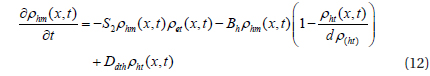
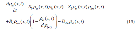
S1,S2,S3,S4: Coefficient of recombination.
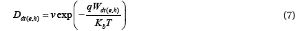
BeBh: Coefficient of trapping of electrons and holes.
De Dh: Coefficient of detrapping of electrons and holes.
[Table 1.] Description of the physical model.

Description of the physical model.
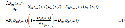
3. DESCRIPTION OF THE MATHEMATICAL MODEL
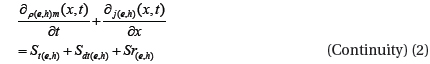
The modeling of transport phenomena is based on solving a system of equations consisting of the equation of continuity and Poisson’s equation. The equations describing the behavior of the charge carriers are as follows, neglecting the diffusion:


E(x,t) and ε are respectively the electric field and the dielectric permittivity of the insulator. The net charge density is local composed of trapped and mobile electrons and holes:

ρet (x,t) and ρht (x,t) : densities of trapped electrons and holes respectively.
ρem (x,t) and ρhm (x,t) : densities of mobile electrons and holes respectively
j(e,h) (x,t) : the fluxes of mobile electrons or holes
St(e,h) : the source term for trapping electrons or holes
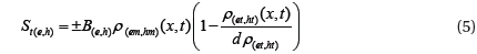
Sdt(e,h) : the source term for detrapping of electrons or holes

Sr(e,h) : the source recombination term

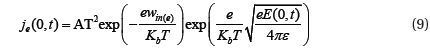
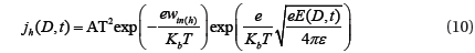
considering that the carriers are injected into the dielectric through the two electrodes, this mechanism is described by the Schottky law.


where: x=0 on the cathode, and x=D (thickness of the dielectric) on the anode. Thuds je(0, t) and jh(D, t) are the densities of electron and hole fluxes to the cathode and anode, respectively, A =1.2 × 10⁶ A.m−2.K−2 is the Richardson constant, win (e,h) are the barriers for the injection of electrons and holes.
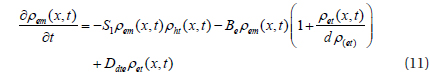
5. EQUATIONS OF THE VARIATION IN CHARGE DENSITIES
There are four types of species:
Variation of mobile electron density:


The local current density for conduction of mobile electrons and holes is written:

The local density of the displacement current is:

The density of the external current is:

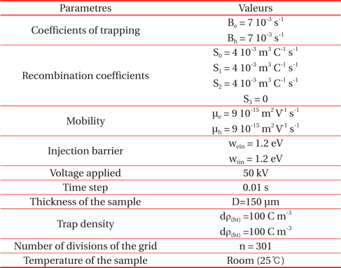
To solve this physical problem, numerical models are accessed by physical variables related to the dynamics of the electric charge. In fact, the finite element method is applied to Poisson’s equation (1) for determining the instantaneous distribution of the electric field. The continuity equation (2) is processed by the Leonard model. A Runge-Kutta high order was applied to equations (11),(12),(13),(14) to obtain better accuracy on the values of the densities of mobile and trapped carriers. To obtain numerical results for the equations and physical conditions, we developed software in Matlab. This software can provide all the distributions relating to electric fields, the net charge density, the densities of mobile and trapped carriers, as well as external current, conduction and displacement. In this part of the work, we consider symmetric parameters for both types of charge carriers(electrons and holes).The result swill be classified according to the intensity of the voltage applied to a low density polyethylene sample (LDPE) with a thickness D of 150 μm. The complementation parameters of the model are summarized in Table 2.
[Table 2.] Parameters and values model.

Parameters and values model.
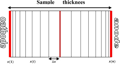
The grid (Fig. 2) computing is discredited in a single direction, and the structure is considered a one-dimensional function of the dielectric thickness(D). This is not uniformly discretized element △x(i) =x(i+1) −x(i) very small near the electrodes.
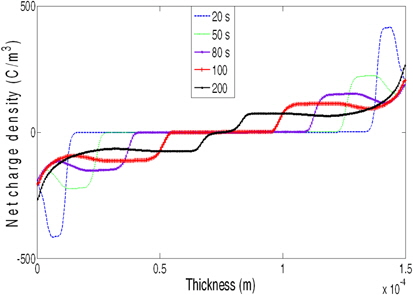
Figure 3 show the net charge density profiles at different time under 50 KV DC voltage. Apparently, we observed the appearance of the packets charges for all profiles at proximity of the electrodes cathode and anode respectively, latest are propagating on the bulk of the sample. During this propagation, we notice the decrease of each packet progressively under the effect of deep trapping. Thus, we notice the increase of velocity of the propagation when increasing the time polarization. we also notice, that all the packets charges either positive and negative charges meet in the middle produced the zone alternance, so that it leads to the beginning of recombination of charge.
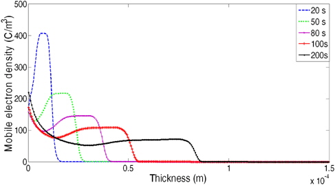
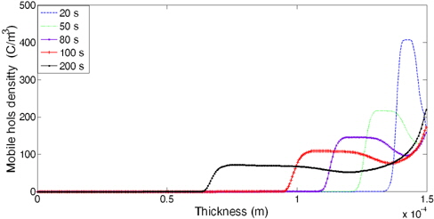
Figure 4 shows the profiles of the absolute values of the densities of electrons mobile profiles at different times under 50 kV DC voltage. We observe that a big number of the mobile electron density close to the cathode forming a lobe, which is the result of negative charge injection. Those charges propagate to words the anode the intensities of these charge packets are weakened due to the trapping of electrons and also their recombination with packets trapped by holes. Recombination is accompanied by an increase of the density of mobile electrons at the cathode .The same process occurs with the density of mobile holes (Fig. 5) at the anode.
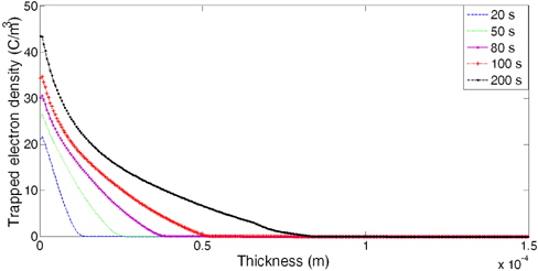
Figure 6 represents the trapped electron density at different time under 50 KV DC voltage. It clearly shows that the trapped electron density increased along with advance of negative packet charge, but not considerable compared with mobile electron charge. In high voltage (more thane 20 KV). The mobile packets charge is much more important than the trapped electron density, thus we can neglect.
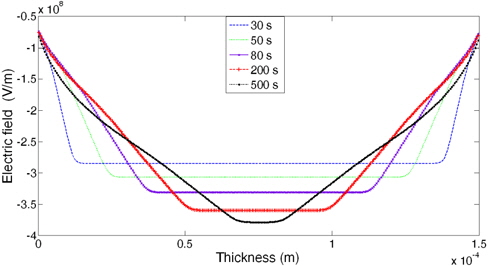
Figure 7 represents electric field distribution of the sample at different time under 50 KV DC voltage. At the beginning of the voltage application , the electric field drops in the vicinity of the electrodes, but in the middle of the sample it increases. This behavior remains until the establishment of the recombination mechanism. The interfacial field is then increased after the recombination at the interfaces.
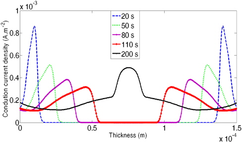
Figure 8 shows the evolution of the instantaneous current in the conduction state as a transitory high voltage of 50 kV. At the beginning of the application of this voltage, the profiles show the appearance of two peaks at the sides of the electrodes, as shown for example at time t=50 s .These maxima are assigned to packets moving loads that are produced under high tension. Furthermore, it appears that during the transitory state, the current conduction patterns show oscillations about a main value that increases with time.
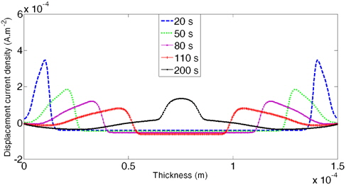
Figure 9 shows profiles of displacement current at different time under 50 KV DC voltages. Which exhibit oscillations around the value zero and at the beginning of the application of the voltage, these oscillations, similar to the conduction current, attenuate gradually to a stationary state in which the displacement current is zero at any point of the polyethylene.
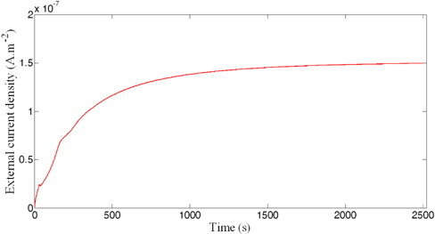
Figure10 shows the evolution of the current density of polyethylene under external applied voltages of 50 kV. In this case, because of the high voltage, the number of mobile electrons and holes generated by intensification of the injection sets the reduction of these costs due to recombination and extraction. Therefore, the current, which is always proportional to the density of the mobile charge, continues to increase until the stationary state.
In this work a first validation of the model, of the symmetrically chosen parameters for both electrons and holes under DC voltage. This validation concerns a voltage of 50 KV at high electric field in low density polyethylene (LDPE). In this model, we notice the appearance packet charge when the electric field is very high , and the mobile charges are the most dominated then the trapped charge density. This high electric field leading to the appearance alternance zone of electron and holes in the middle of polyethylene, which becomes more and more important as the voltage is very higher.