In this paper, we present simulation results obtained using SILVACO TCAD tools for a 3-D silicon on insulator (SOI) n-FinFET structure with a gate length of 8 nm at 300K. The effects of variations of the device’s key electrical parameters, such as threshold voltage, subthreshold slope, transconductance, drain induced barrier lowering, oncurrent, leakage current and on/off current ratio are presented and analyzed. We will also describe some simulation results related to the influence of the gate work function variations on the considered structure. These variations have a direct impact on the electrical device characteristics. The results show that the threshold voltage decreases when we reduce the gate metal work function Φm. As a consequence, the behavior of the leakage current improves with increased Φm. Therefore, the short channel effects in real 3-D FinFET structures can reasonably be controlled and improved by proper adjustment of the gate metal work function.
The trend in miniaturization of electronic components and transistors in integrated circuits has dramatically increased over the past thirty years. The goal is to integrate more components per unit area and, thus, improve circuit performance while lowering their manufacturing cost as predicted by "Moore’s Law".
Major semiconductor companies introduced the use of silicon on insulator (SOI) substrate in manufacturing microprocessors to minimize parasitic capacitances and to improve current drive, circuit speed and power consumption [1].
Among the important parameters, which are related to CMOS scaling, the gate length plays a fundamental role. Intel plans to achieve Fin-Shaped Field Effect Transistor (FinFET) technology 10 nm devices in 2015 and 7 nm devices in 2017. Eventually, it will be as low as 1 nm; it will be so small that the quantum physics effects will become relevant [2].
The multi-gate transistors like FinFETs are considered to be the best candidates to extend the use of CMOS technology beyond the barrier of 14 nm. As with classic CMOS technology, the design of integrated circuits requires the availability of high performance and predictive compact models of these devices.
In this work, we study the device structure SOI n-FinFET with an 8 nm gate length by keeping in mind either speed and power consumption as major targets. The region between the source and the drain of the analyzed device is covered by implementing the high-k gate dielectrics (Si3N4), which allows further miniaturization of electronic components. In the simulation, the Lombardi constant voltage and temperature (CVT) and the ShockleyRead-Hall (SRH) models were considered. We also study the influence of variation of the gate work function on the most important parameters, such as threshold voltage (Vth), subthreshold slope (SS), transconductance (gm), drain induced barrier lowering (DIBL), on-current (Ion), leakage current (Ioff), and the on/off current ratio of nanoscale FinFETs.
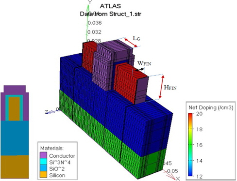
The schematic structure used for the simulations is represented in Fig. 1. The different parameters of the considered structure are assumed as follows in Table 1:
[Table 1.] Parameters of symmetrical SOI n-FinFET
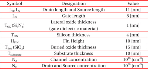
Parameters of symmetrical SOI n-FinFET
The FinFET technology is based on vertical silicon fin characterized by the fin length (LG), fin height (HFIN), and the silicon thickness (WFIN) as shown in Fig. 1 [3].
3. 3-D DEVICE SIMULATION USING SILVACO-ATLAS
The software package Silvaco-Atlas was used to construct, examine, and simulate the structure and characteristics of the FinFET device in three dimensions.
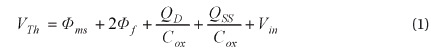
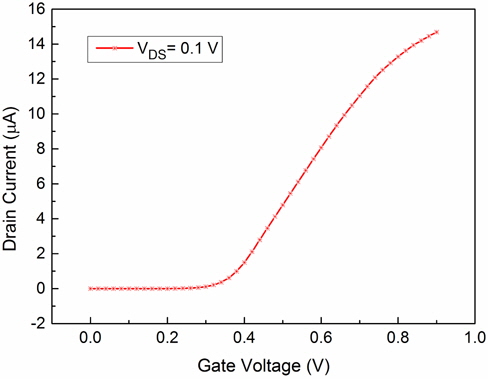
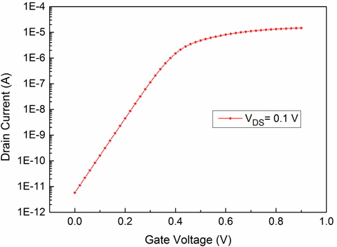
In Figs. 2 and 3, IDS-VGS transfer characteristics are shown on a linear scale and log scale for an SOI n-FinFET device structure. In Fig. 2, it is observed that the threshold voltage of an SOI nFinFET is 0.31 V at VDS = 0.1 V. The threshold voltage expression in case of a MultiGate Field-Effect Transistor (MuGFET) device structure can be expressed as [1]:


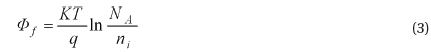
Where Qss represents charge in the gate dielectric, Cox is the gate capacitance, QD is the depletion charge in the channel, Φms represents the metal-semiconductor work function given by the difference between the gate metal work function Φm and the semiconductor work function Φs, Φf is the Fermi potential, which, for P-type silicon, is given by:

Where k is the Boltzmann constant, T is the temperature, q is the electron charge, NA is the acceptor concentration in the p-substrate, and ni is the intrinsic carrier concentration. The value of kT/q is 0.02586 V at T = 300 K.
The transconductance gm quantifies the drain current variation with a gate-source voltage variation while keeping the drainsource voltage constant [4,5]:
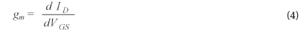
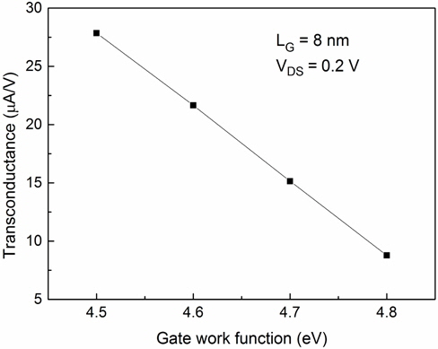
Therefore, the value of gm is extracted by taking the derivative of the IDS-VGS curve (Fig. 2). The value obtained is 16.14 μA/V at VDS = 0.1 V.
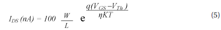
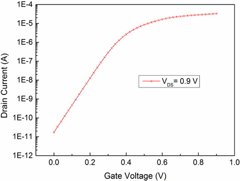
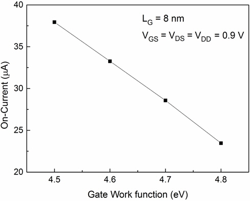
The threshold voltage (Vth) is a very important parameter for obtaining a higher on-state current, which improves the circuit speed. In Fig. 4, it is observed that the on-state current output is 33.26 μA at VGS = VDS = VDD and VDS = 0.9 V, where VDD is the supply voltage. Furthermore, IDS is calculated as reported in [4,5]:

[Fig. 3.] IDS-VGS characteristics on a log scale for an SOI n-FinFET with Φm = 4.6 eV at VDS= 0.1 V.

[Fig. 4.] IDS-VGS characteristics on a log scale for an SOI n-FinFET with Φm = 4.6 eV at VDS= 0.9 V.

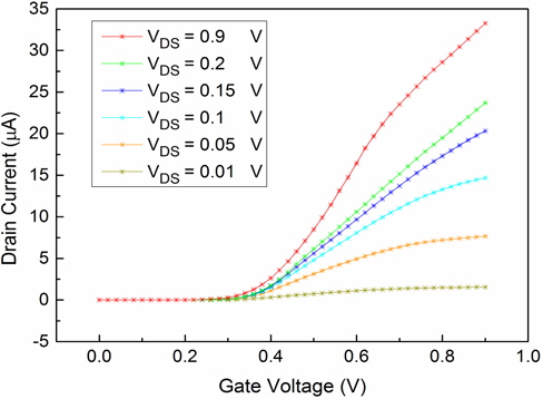
As the drain voltage is increased, the average velocity of the electrons flowing from the source to the drain increases at a given VGS value. From Fig. 5, it is observed that upon raising the gate voltage above the threshold voltage, the conductance increases. As a result, a larger current will flow when the gate voltage is greater than the threshold voltage and the drain voltage is increased
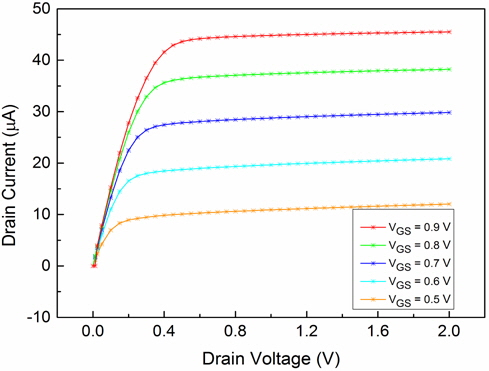
The drain current versus drain voltage is plotted in Fig. 6. The effect of the gate voltage on the output characteristics (IDS-VDS) was also observed. The results obtained clearly show a good saturation region of the device at a higher gate bias.
The subthreshold slope (SS) is the major parameter for calculating the leakage current. Furthermore, SS is calculated as in [4,5]:
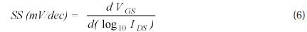
A typical value for the SS parameter of a MuGFET is 60 mV/decade, (i.e., a 60 mV change in gate voltage brings about a tenfold change in drain current) [4,5]. The subthreshold slope is 69.13 mV/decade in the considered n-FinFET device at VDS = 0.1 V.
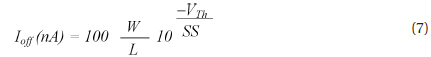
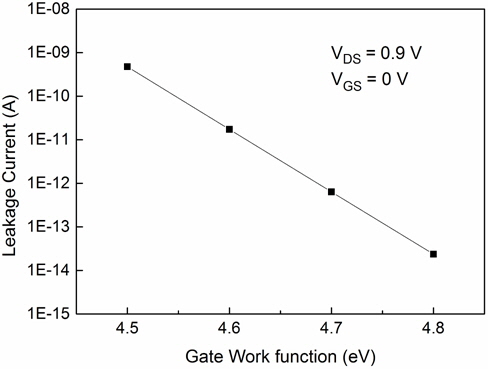
The leakage current is directly related to the SS. Fig. 4 shows, that the leakage current output Ioff is 17.3 pA at VGS = 0 V and VDS = 0.9 V. Ioff has been calculated by the following formula in [4,5]:

The leakage current and on-current of the considered device (i.e., 17.3 pA and 33.26 μA) are improved compared with the results of the recent paper reporting on a 16 nm n-type FinFET (i.e., 164 pA and 31.6 μA) [6]. The lowering of Ioff is a valuable result in order to minimize the static power dissipation even when the device is in the standby mode. The ratio Ion/Ioff exceeds 106 , which indicates the excellent on-state and off-state characteristics
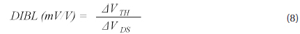
The value of the drain induced barrier lowering (DIBL) is calculated by using the relation reported in [4, 5]:

The DIBL is defined as the difference in threshold voltage when the drain voltage is increased from 0.01 V to 0.05 V. In our case, DIBL is 85.30 mV/V for the SOI n-FinFET at a gate length of 8 nm as shown in Fig. 7.
4. EFFECTS OF VARIATIONS OF THE GATE METAL WORK FUNCTION
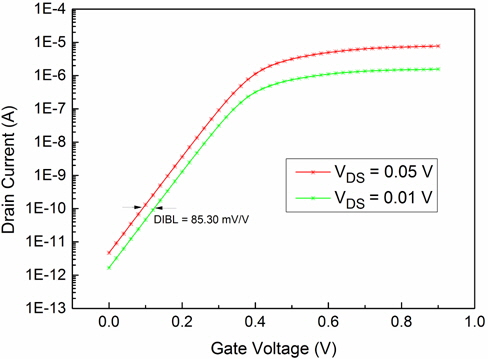
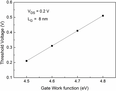
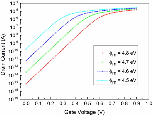
It is very useful to consider the impact of the gate metal work function Φm on the device current and performances. Fig. 8 illustrates the transfer characteristics when Φm is increased from 4.5 eV to 4.8 eV in the considered device. We can observe that when the gate work function increases, the threshold voltage increases and the drain current characteristic slope decreases as shown in Figs. 8~10.
In Fig. 11, it is observed that the subthreshold slope does not change with the variation of the gate work function. According to the relationship between Ioff and Vth reported in eq. 7, the threshold voltage increases with a higher metal gate work function, which in turn causes a reduction in the leakage current as shown in Fig. 12.
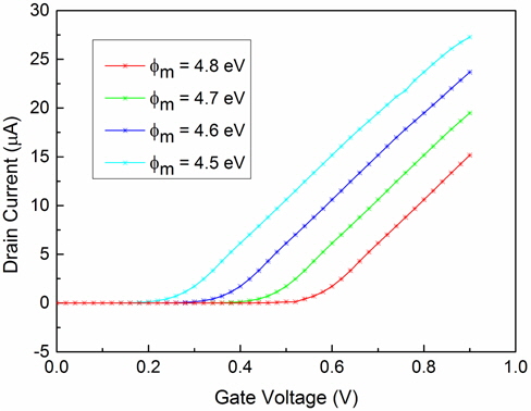
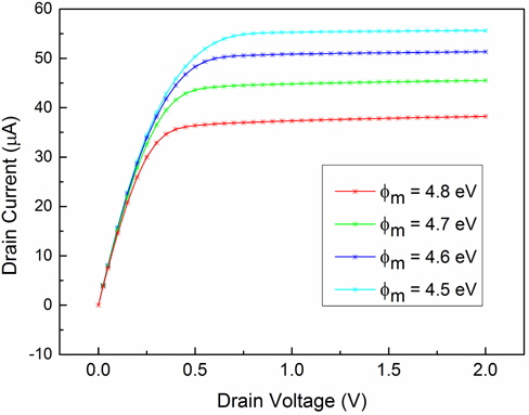
From Fig. 13, we can notice that the on-current decreases as Φm is increased and again, as shown in Fig. 14, the on/off current ratio improves with an increase of Φm.
Figure 15 shows that a low value of the gate metal work function leads to a higher gm value, and a higher drain current as shown in Fig. 13. According to the relationship in eq. 4, gm is directly related to the drain current (Id). Therefore, we can conclude that the work function has a very notable effect on the threshold voltage, the transconductance, the leakage current, the on-current and the on/off current ratio.
In this work, we have used the numerical simulation tool Atlas Silvaco to construct, examine, and simulate a new SOI n-FinFET with a gate length of 8 nm. As indicated by the three-dimensional simulation results, we found that the short-channel effect (SCE) in SOI n-FinFET can be reasonably controlled and improved by proper adjustment of the metal gate work function. An increased value of Φm improves the leakage current and on/off current ratio, but causes a rise of the threshold voltage and a reduction of the device on-current and transconductance as well.
Therefore, this nanometer gate device has shown that it provides improved control of the channel, allowing more efficient reduction of the leakage current at a gate length of 8 nm. We feel confident that the work function will also confirm its strong and positive impact on the electrical device characteristics of multiple-gate MOSFETs to be studied with the same procedure and tool.