This research proposes the use of a composition modulated (ZrO2)x(Al2O3)1-x film as a charge trapping layer for charge trap flash memory; this is possible when the Zr (Al) atomic percent is controlled to form a variable bandgap as identified by the valence band offsets and electron energy loss spectrum measurements. Compared to memory devices with uniform compositional (ZrO2)0.1(Al2O3)0.9 or a (ZrO2)0.92(Al2O3)0.08 trapping layer, the memory device using the composition modulated (ZrO2)x(Al2O3)1-x as the charge trapping layer exhibits a larger memory window (6.0 V) at the gate sweeping voltage of ±8 V, improved data retention, and significantly faster program/erase speed. Improvements of the memory characteristics are attributed to the special energy band alignments resulting from non-uniform distribution of elemental composition. These results indicate that the composition modulated (ZrO2)x(Al2O3)1-x film is a promising candidate for future nonvolatile memory device applications.
With conventional nonvolatile flash memory devices approaching their scaling limitation, tremendous effort has been made to explore the next generation nonvolatile solid state memory devices for use in mobile electronics such as digital cameras, MP3 players, and mobile phones [1-5]. Among the family of nonvolatile memories, the charge trap flash memory (CTFM) is one of the most promising candidates due to its advantages such as better scalability, low power, and process simplicity [6]. Nevertheless, one problem in a conventional CTFM device with an Si3N4 trapping layer is the small potential barrier, which leads to poor retention characteristics. Since the Si3N4 based CTFM device faces the challenge of the trade-off between data retention and program/erase speed [7]. In order to further improve memory characteristics and achieve the trade-off among the memory window, program/erase speed and data retention, extensive research has been carried out in recent years. This research has involved the use of nanocrystals (e.g., Ge [8], Si [9], Ni [10], and NiSi [11]), stacked structure [12-14], binary oxide dielectric film (e.g.,HfO2 [15], GdO [16], and ZrO2 [17]), and multiple oxide dielectric film [18,19] as a charge trapping layer. This work proposes a bandgap engineering technique using a composition modulated (ZrO2)x(Al2O3)1-x film as the charge trapping layer in the CTFM device to improve the memory characteristics. This involves the formation of a variable bandgap due to the non-uniform distribution of elemental composition in the charge trapping layer causing different energy band offsets.
P-type Si (100) substrates with a resistivity of 3~20 Ω cm were cleaned by the standard Radio Corporation of America process to remove native oxide. Then a 3 nm Al2O3 film (30 deposition cycles) as the tunneling oxide (TO) was deposited by atomic layer deposition (ALD) using trimethylaluminium Al(CH3)3 precursors at a substrate temperature of 300℃. Following that, a 10 nm composition modulated (ZrO2)x(Al2O3)1-x film (denoted as CM-ZAO) was deposited as the charge trapping layer by ALD using ZrCl4 and Al(CH3)3 precursors, and O3 vapor served as the oxygen source. The ratio of Zr (Al) in the charge- trapping layer first increased (decreased) and then decreased (increased) by controlling the number of ALD deposition cycles. In the process, we deposited 10 units, and every 10 cycles including Al2O3/ZrO2/Al2O3 were a unit. We successively deposited Al2O3/ZrO2/Al2O3 with different cycles in every unit, and the numbers are 5/2/3, 4/3/3, 3/5/2, 2/6/2, 1/8/1, 2/6/2, 2/5/3, 3/3/4, 3/2/5, and 7/2/1 to realize nonuniform distribution of elemental composition. Subsequently, a 12 nm Al2O3 (120 deposition cycles) was deposited by ALD as the blocking oxide (BO). A post deposition annealing process was carried out at a temperature of 900℃ for 30 s in N2 ambience. Finally, Pt gate electrodes with an area of 7.85 × 10⁻⁵ cm2 were formed by a magnetron sputtering technique, and the silver glue was then spread on the side of the Si substrates to act as the bottom electrodes. The above fabricated memory device was labeled as S1, and the structural schematic diagram was shown in Fig. 1(a). To confirm the role of the CM-ZAO film, control samples with single uniform 10 nm (ZrO2)0.1(Al2O3)0.9 or (ZrO2)0.92(Al2O3)0.08 as the charge trapping layer were simultaneously fabricated, which were named S2 and S3, respectively. In the process, ZrCl4 and Al(CH3)3 precursors, and O3 vapor served as an oxygen source were used to deposit the (ZrO2)0.1(Al2O3)0.9 and (ZrO2)0.92(Al2O3)0.08 films. We deposited 10 Al2O3/ZrO2/Al2O3 units, and the number of cycles in every unit was 5/1/4 and 1/4/1, respectively. The precursor temperatures were kept at 180℃. The X-ray photoelectron spectroscopy (XPS) was used to investigate the elemental composition and energy band alignment of the memory devices. The selected area electron diffraction (SAED) pattern and cross-sectional microstructures of the device were examined by transmission electron microscopy (TEM). The electrical characteristics of the memory devices including memory windows, program/erase speed and data retention characteristics were analyzed by the Keithely 4,200 semiconductor characterization system.
Figure 1(b) is the cross sectional TEM image of the S1, which shows distinct interfaces between the TO, CM-ZAO and BO. Meanwhile, the SAED was performed in the region of the CMZAO, as shown in the inset of Fig. 1(b), and there was no diffraction spot. The results demonstrated that the CM-ZAO was still in an amorphous state after rapid thermal annealing treatment at 900℃ for 30 s in N2 ambient.
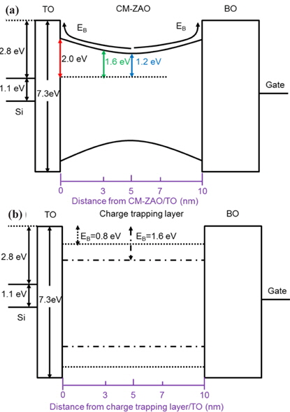
Since the elemental compositions play a key role in energy band alignment of memory devices [20], it is important to analyze the composition’s distribution in the charge-trapping layer for S1, S2, and S3. During the process, the memory structures were etched from BO to TO layer by using Ar+ beam sputtering to detect the XPS signals, and the etch rate is 1 nm/min. The position of the CM-ZAO/BO (TO/CM-ZAO) interface was confirmed until the signal of Zr element appear (disappear). Table 1 shows the atomic percent (at.%) distribution of Zr and Al as well as an x value in the charge-trapping layer for the three samples. The Zr (Al) at.% first increases (decreases) and then decreases (increases), and the maximum (minimum) value appears at the middle of the CM-ZAO for S1. It is worth noting that the elemental compositions show almost symmetrical distribution on both sides of the middle position of CM-ZAO. Nevertheless, for S2 and S3, the Zr (Al) at.%, which respectively corresponds to TO/CMZAO and the middle of CM-ZAO in S1, is almost constant in the charge-trapping layer. Based on the above results, we measured the valence band spectra and O1s electron energy loss spectra by XPS at four positions (TO/Si interface, CM-ZAO/TO interface, from CM-ZAO/TO 3 nm and middle of CM-ZAO) in order to obtain the energy band alignment of the S1.

Elemental compositions in the distribution in the charge trapping layer for S1, S2, and S3 samples (measured from the TO/charge trapping layer to the charge trapping layer/BO interface) estimated by XPS. The ZrO2 mole fraction value x are also given in the table, where The Zr at.%=x/(5-2x) and the Al at.%=2(1-x)/(5-2x).
The valence band maximum (VBM) of the cleaned Si surface is determined to be by using the linear extrapolation method [21] as shown in Fig. 2(a). Using the same method the VBM at the above four positions were 3.8 eV, 3.3 eV, 2.9 eV, and 2.3 eV, respectively. Therefore, the valence band offset (VBO) that is relative to the Si substrate was calculated as 3.4 eV, 2.9 eV, 2.5 eV, and 1.9 eV by using formula for the above measured positions, respectively. The band gap (Eg) of TO was determined to be 7.3 eV by the onsets of O1s electron energy loss spectra collected at the interfaces of the TO/Si interface, as shown in Fig. 2(b). Similarly, the bandgaps at CM-ZAO/ TO, from CM-ZAO/TO 3 nm and the middle of CM-ZAO were 6.0 eV, 5.2 eV, and 4.2 eV, respectively. Therefore, using the formula of the calculated value of the conduction band offset (CBO) at TO/Si, CM-ZAO/TO, from CM-ZAO/TO 3 nm and the middle of CM-ZAO were 2.8 eV, 2.0 eV,1.6 eV, and 1.2 eV, respectively, where is 1.1 eV. According to the composition of the symmetric distribution around the middle of the CM-ZAO film, the energy band alignment of the S1 was schematically depicted in Fig. 3(a). The bandgap of CM-ZAO is determined by the Zr and Al content in the film, which monotonously decreases with increasing Zr content, or increases with decreasing Al content. Therefore, the potential barrier EB between TO and CM-ZAO (BO and CM-ZAO) is variable and in the range of 0.8 to 1.6 eV. By comparison, the charge-trapping layer has a uniform elemental composition distribution resulting in a changeless potential barrier for S2 and S3, as shown in Fig. 3(b).
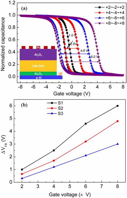
Figure 4(a) shows high frequency (1 MHz) C-V hysteresis of S1 with different gate sweeping voltages to observe its charge storage effect. The C-V curves exhibit an obvious memory window (1 V) in a small sweeping range of ±2 V. When the gate sweeping voltage range is increased to ±8 V, a significant memory window of 6.0 V can be observed. In addition, the flatband voltage shift (ΔVFB) of the S1, S2, and S3 are shown in Fig. 4(b), in which relatively large ΔVFB are observed under the same gate sweeping voltages for S1, indicating that a tremendous amount of electron traps exist in the charge-trapping layer of S1 compared to the charge-trapping layer of S2 and S3.
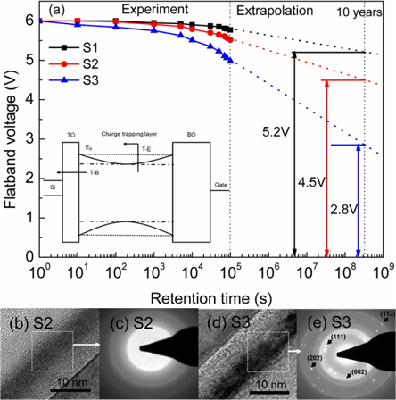
We programmed S1, S2, and S3 with an identical initial flatband voltage (6 V) to compare their data retention characteristics at room temperature, as shown in Fig. 5(a). S1 exhibited a slight decrease in flatband voltage, whereas S2 and S3 show obvious charge loss after 1.0 × 10⁵ s, especially for S3. In order to predict the data retention characteristics for a long time, we extrapolated the experimental data for up to 10 years. The results indicate that the decrease in the memory window from the initial 6.0 V to 5.2 V, 4.5 V, and 2.8 V, and the window losses are about 13.3%, 25%, and 53.3% for S1, S2, and S3, respectively. It is known that T-B tunneling and T-E are the important charge loss mechanisms, as shown in inset of Fig. 5(a). At room temperature, the T-B tunneling process is the dominant charge loss mechanism, and can be reduced by increasing the potential barrier EB [22,23]. Though the chargetrapping layer of S2 is an amorphous state (Fig. 5(b) and (c)), the smaller EB (0.8 eV) cannot effectively maintain the trapped electrons, which are easily lost via T-B tunneling. Instead, S3 with a maximum EB (1.6 eV) shows the worst retention performance due to the crystallization of (ZrO2)0.92(Al2O3)0.08 charge-trapping layer after post annealing treatment, as shown in Fig. 5(d) and (e). The crystallization of the film will generate grain boundaries, which can act as current leakage paths [18]. The excellent data retention characteristics of S1 should be attributed to the amorphous charge trapping layer [24] and variable potential barrier EB (0.8 to 1.6 eV), which suppress the leakage of trapped electrons toward the tunneling and blocking oxide.
Figure 6(a) and (b) show the transient program/erase characteristics of S1, S2, and S3 memory devices. The samples are charged at ±8 V by a single electrical pulse with different width. It is observed that S1 exhibits a faster program and erase speed than S2 and S3. For example, the program times at a memory window of 1 V for S1, S2, and S3 are 2 × 10⁻⁶ s, 2.2 × 10⁻⁵ s and 6.8 × 10⁻⁴ s, respectively. The results can be explained by the energy band diagram shown in Fig. 3. In a program state, the CBO of CM-ZAO with respect to Si is variable (1.2 to 2.0 eV) in S1, compared to identical CBO 2.0 eV for (ZrO2)0.1(Al2O3)0.9 in S2. Hence, at the same gate bias voltages, the electron tunneling distance from the Si substrate to the conduction band of the charge-trapping layer is shorter in CM-ZAO and longer in (ZrO2)0.1(Al2O3)0.9. Moreover, the injected electrons are also reduced through blocking oxide into the gate due to the large potential barrier EB, resulting in a faster program speed for S1 [25]. For the erase case, similar to the program state, the variable VBO (2.9 to 1.9 eV) and large potential barrier result in a faster erase speed for S1 compared to S2. As mentioned above, the poor program and erase speed of S3 should be attributed to the crystallization of the charge-trapping layer.
In summary, a charge trap flash memory with the composition modulated (ZrO2)x(Al2O3)1-x charge trapping layer, Al2O3 tunneling oxide, and Al2O3 blocking oxide has been fabricated and investigated. We have demonstrated that the composition modulated (ZrO2)x(Al2O3)1-x charge trapping layer can simultaneously satisfy a larger memory window, faster program/erase speed, and excellent data retention. The results are attributed to the special energy band structure of the trapping layer. Based on this work, the charge trap memory device with composition modulated (ZrO2) x(Al2O3)1-x trapping layer may be a potential candidate for future nonvolatile flash memory device applications.