Solder is a metal substance having a low melting point of about 200℃. The soldering iron is used to heat the solder using a certain temperature until it melts. The purpose of melting the solder is to use it to join other metals together, which is known as a copper track or component leads when it is solidified again in an electronic study [1].
Nowadays, solder is widely used in the electronic packaging industry, and to establish an electrical connection between parts in the circuit by using molten metal and a soldiering iron [2]. Solders are also used in electronic devices and typically thaw at temperatures beneath 350℃.
Eutectic solder consists of 37% lead (Pb) and 63% tin (Sn). Generally, it is known as 63/37 solder and is preferred as when it is melted, it changes right away from solid to liquid state [3]. Intermetallic and covalent bonds are formed from the reaction between solder and a small quantity of the base metal. The intermetallic compound (IMC) is a chemical compound that develops and grows between the metals existing in the base metal, protective platings and solder. Its formation is essential for an excellent solder connection. However, the excessive formation of IMCs results in fragility [4].
Tin-lead solder alloys are used extensively in the microelectronic industries. The usage of tin-lead became popular due to its low price, high wetting properties and average melting point temperature [5]. There is no requirement for high temperatures.
Unfortunately, researchers have found that lead can be hazardous to the environment and to human health, and solder based lead containing toxic [5]. Lead solders could affect human health as lead causes deterioration of the central neural systems and the blood. If Pb particles are inhaled or ingested they will then accumulate in the human body and may cause health risks [6].
Conversions to lead-free alternatives are being considered for several reasons, including health concerns, enormous thermal stresses of elements, and with the increasing use of temperaturesensitive elements and substrates. The most appropriate Pb-free solder alloys are those based on tin and containing copper and/or silver [7].
This work uses a lead-free solder alloy. Tin-silver-copper (Sn/Ag/Cu) solder is widely known by the acronym “SAC”. SAC solder is generally considered as eutectic or nearly eutectic at a temperature of almost 217℃ [8]. Its defrosting stage is 221℃ and 227℃, both of which are beneath the melting point of the eutectic tin-3.5 silver (wt. %) and the eutectic tin-0.7 copper solders, which are commonly known by the acronyms Sn-3.5Ag and Sn-0.7Cu [9].
Generally, the range of composition of SAC alloys is from 0.5 to 0.8% for copper, 3.0 to 4.0% for silver, and the rest of the composition is an Sn alloy [8]. According to Grusd, and in contrast to tin-40lead (Sn/40Pb), Pb-free solders of the combination tinsilver-X offer better slink resistivity at 100℃ and room temperature [10].
The intermetallic compound (IMC) layer starts to develop and grow as the temperature increases. It grows faster when the temperature is high. During the soldering process, the foremost IMC formed is Cu6Sn5. However, for the reaction between Cu and Cu6Sn5, a very slim film of Cu3Sn is formed at the surface [10].
Generally, it is reported that the IMC layer formed on leadfree solder is slightly thicker than the IMC layer formed when a eutectic SnPb solder is used. When an Sn-Ag lead-free solder is used, the IMC layer formed is thinner compared to PbSn. However, in certain cases it is found that the IMC formed is 2~3 times thicker than eutectic PbSn [11].
This paper reports the results of an investigation of the microstructural features, contact angle as well as the thickness and formation of IMCs for varying aging times, using SAC 305 solder. Results show that this solder is suitable for use in industry as the IMC formed is not too thick and the contact angle is less than 90°. Since the technology depends on the formation of intermetallic compounds, it is important to identify and control its growth, to hinder any disadvantageous effects on the solder joints.
A printed circuit board with SAC 305 lead-free solder was prepared. SAC 305 lead-free solder comprises 96.5% Sn, 3% Ag and 0.5% Cu [12] and was reflowed at a temperature 215℃ for eight seconds. These samples (SAC 305) were cut into eight smaller pieces using a diamond blade cutter with model Micracut 150 precision cutter, and were divided into four big solder and four small solder.
Before they were examined by optical microscope for thicknesses and contact angles, the samples were firstly ground and polished and mounted. All the samples were ground using 24000 grit SiC paper to prepare the surface flatness, and polished to remove any excess using abrasive silicon carbide sandpaper with a smooth surface of 2400. An 0.05 um polishing pad was used to polish the samples. A Forcipol 2 Grinder-Polisher machine was used to grind and polish the samples.
An optical microscope was then used to observe the microstructures of the samples. By using an optical microscope, the contact angle of each sample, the thickness of the solder and IMC and also the substrate are measured. The wetting angle of the solder on the substrate was determined by measuring the contact angle. The thickness of intermetallic compound and contact angle were measured by the microscope with the aid of analytical software (Visver 3.3 (Professional) at 20x magnification). In order to use the analytical software, a scale had to be defined so that measurement results can be presented in calibrated units, such as millimeters. In order to set the scale, the straight line selection tool was used to make a line selection that corresponds to a known distance.
The aging process measurements were conducted at 24, 48, and 72 hours duration. Temperature for the aging process was fixed at 30℃. Specimens then were mounted in epoxy resin, mechanically ground and polished using a 1.0 um polishing pad to observe the interface between the solder and substrate, and to remeasure the IMC thicknesses and contact angles.
In this research, the thickness of the IMC layers and contact angles were taken as an average over three magnifications, which were 5x, 10x, and 20x. The average thickness was calculated by dividing the total length of the image.
The formation of intermetallic compound between solder and copper substrate was measured using XRD analysis. XRD equipment used in this study was XPERT-PRO by PANalytical with monochromatic Cu kα radiation. Diffractograms generated in XRD measurement were analyzed using XPERT-PRO High Score Plus software.
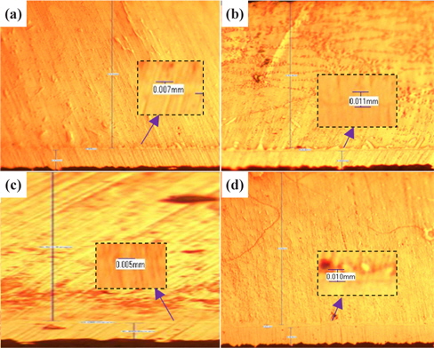
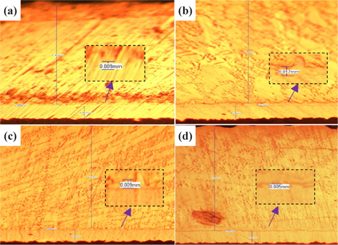
Figure 1 presents the results of the investigation of the thickness of IMC at the four duration times with 30℃ for SAC 305 solder.
From Fig. 1 and Table 1, it can be observed that the thickness of the IMC layer increased after the aging process due to the thick formation of Cu6Sn5 and Cu3Sn on the interface. The IMC thickness increased from 0.005 to 0.008 mm. This is due to the increase in the formation of Cu6Sn5 and Cu3Sn when the sample is exposed to high temperatures during the aging process.
[Table 1.] Average thicknesses for big solder.

Average thicknesses for big solder.
However, the thickness at 48 hours aging time is much lower than that at 24 hours. This finding may be attributable to the increment of crack length as the aging time increase. The thickness of the IMC decreases as the length of crack increases. This is supported by Jen, Chiou and Yu in their journal [13]. An IMC with defects such as voids and cracks happens after exposure to aging. This is agreed by Raoeslison, Racine, Zhang, and Buirona in their journal [14].
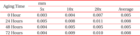
Figure 2 presents the results of the investigation of the thickness of IMC for small solder at the four duration times with 30℃ for SAC 305 solder.
From Fig. 2 and Table 2, the changes to the IMC layer thickness after the aging process can be observed. The thickness of IMC surged from 0.005 mm to 0.008 mm after 24 hours aging, but at 48 hours its thickness had increase by 0.001 mm only, compared to its thickness at time zero. The thickness of intermetallic compound is surged when the aging time increased from zero to 24 hours. This condition happened because of the superior solid state reaction and is also supported by Niwat and Kannachai [14]. Even though only a small amount of solder is used, the IMC still grows when it is exposed to high temperature during the aging process. According to Raoeslison, Racine, Zhang, and Buirona, IMC may form even with a very little thickness like a micrometer thick [15].
[Table 2.] Average thicknesses for small solder

Average thicknesses for small solder
The increase in the thickness of IMC indicates the presence of small Cu6Sn5 at the interface of solder and copper substrates. A Cu6Sn5 layer formed during the reaction at the Sn-based solder and Cu interface. After 72 hours, the thickness of IMC has not increased, probably because of the decrease in the thickness of Cu6Sn5 due to the initial development of Cu3Sn at the alloy’s surface. Niwat and Kannachai reported that the thickness of Cu6Sn5reduced as Cu3Sn forms at the expense of Cu6Sn5 [16].
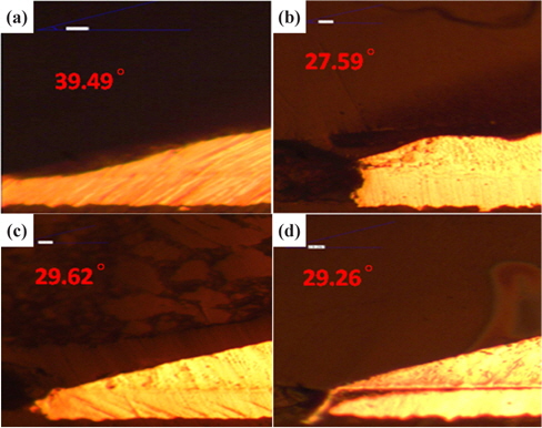
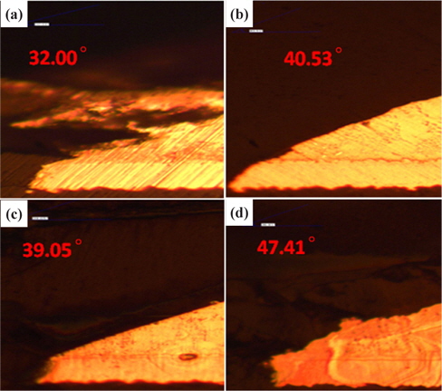
The wettability of the solder on the Cu substrate can be determined by the contact angle of the solder on the substrate, as shown in Fig. 3. As the aging time increased from zero to 72 hours, a significant decrease was seen in the contact angle of the solder on the substrate. The reduction of contact angle with increasing reflow temperature may be attributed to the increase in the reaction rate of the flux. For a smaller contact angle, better wetting behavior can be obtained.
The decrease in the contact angle is due to the defects at the interface of the substances, formation of IMC such as Cu6Sn5 and Cu3Sn, as well as due to the increase in the area of solid metal contact. This statement is strongly supported by Eustathopoulos, Nicholas, and Drevet [18]. Since the contact angle between the solder and substrate in the investigated aging range is much lower than 90° it can be concluded that the solderability of this solder is good.
Figure 4 presents the contact angles of IMC for small solder at the four duration times with 30℃ for SAC 305 solder. It can be observed that the contact angle slightly increases after the aging process. This is due to the adsorption of oxygen on solid substrates. All the contact angles obtained after the aging process are below 90°.
Any contact angle below 90° is considered small, which correspond to excellent wettability. High wettability indicates that the solder joint is good. This statement is strongly supported by Yuan and Lee [15].
According to Suganuma, it is possible for two types of IMC, Cu6Sn5 and Cu3Sn, to be formed between an Sn alloy and a Cu substrate at temperatures lower than 350℃.
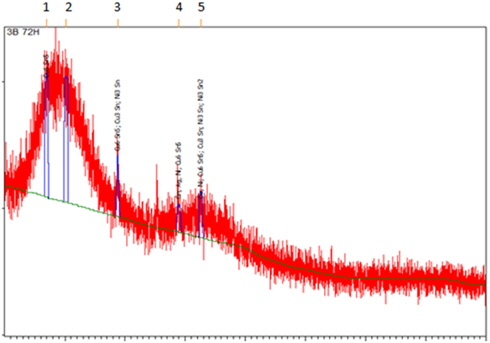
The presence of Cu6Sn5 (ICDD 03-065-2303) and Cu3Sn (ICDD 01-071-7870) was confirmed by XRD analysis (Fig. 5). A Cu3Sn layer is usually formed at high temperature. The formation of these IMCs may be attributable to the saturation of molten solder in contact with Cu. The distribution pattern of IMC is different due to the movement and distribution of atoms during the aging process.
Besides, through this analysis also, nickel (Ni) was also found to exist in the sample. Thus, Ni3Sn2 (ICDD 03-065-9459) and Ni3Sn (ICDD 01-072-2560) are formed from the reaction between solder and Ni substrate.
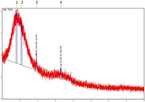
Figure 6. shows the XRD diffractogram obtained from XRD analysis. Cu6Sn5 (ICDD 03-065-2303), Cu3Sn (ICDD 01-071-7870) and Ni3Sn (ICDD 03-065-9703) IMC layers were confirmed present in the sample. The formation of the Cu6Sn5 layer occurred after the liquid solder spread to the existing Cu3Sn layer.
The IMC formation is mainly because of the movement of the electrons inside atoms due to high temperature and the diffusion that takes place during the aging process. The diffusion is mathematically investigated by Fick’s law [16]. Temperature affects the diffusion coefficients which describe how fast the diffusion can occur. This is supported by Fan, Thomy and Vollersten in their journal [17].
The wettability and microstructural characteristics of SAC 305 lead-free solder were investigated. It can be concluded that the solderability of this solder is good when the contact angle between the solder and substrate in the investigated aging range is much lower than 90°.
The IMC thickness and contact angle of the solder on Cu were evaluated for 0, 24, 48, and 72 hours aging time. As the aging time increased, the IMC thickness was found to increase. A reduction in contact angle in this sample after the aging process improved wettability was observed as the temperature increased.
The intermetallic compounds in the SAC 305 solder are Cu6Sn5, Cu3Sn, Ni3Sn and Ni3Sn2. The Cu6Sn5 inter metallic compound already existed in the sample, before aging. Ni3Sn, Ni3Sn2 and Cu3Sn were formed after the aging process. Their formation was in the form of a reaction product between Sn solder alloy and Cu substrate. The free Cu atom diffuses through the Sn solder atom and produces Cu3 Sn. The thickness of Cu6Sn5 increases because of the formation of Cu3Sn at the surface of Cu6Sn5.