Amorphous oxide semiconductors (AOSs) are promising candidate for the next generation semiconductor materials. Oxide TFT have shown good electrical properties such as high field effect mobility, low subthreshold slope, and high carrier concentration, which were comparable to hydrogenated amorphous silicon (a-Si) TFT.[1-4] Amorphous oxides are composed of heavymetal cations, which constitute attractive compound. However, the presentation of the second metal ion in the main matrix enhances the film’s intensity to oxygen that can control electrical properties. [5] Conventional a-Si is inappropriate for large-area ultra-definition (UD) and 3-dimensional (3D) displays, due to low field effect mobility, and it hardly adapts large size display. In the past decade, AOSs have made tremendous improvement in display industry. Traditional deposition process for oxide semiconductor, such as physical vapor deposition (PVD), chemical vapor deposition (CVD), or pulsed laser deposition (PLD) require vacuum process, which has high manufacturing cost and low-throughput.[6-9] Many effort have been reported by high-performance oxide TFTs using solution process which has a simple, low cost, and high throughput. Several solution processes have been developed for oxide semiconductors, such as spin coating, dip coating, and inkjet printing. These characteristics have been used in various device applications, such as flexible displays, transparent displays, and large size display. However, there are still many challenges that impede the field effect mobility due to the trap state. There have been intensive explorations of new multicomponent oxide semiconductor by using solution process. In order to decompose the organic solvent and residual materials, solution process generally needs a high annealing temperature. SIZO TFT shows good transfer characteristics at 300℃ annealing temperature. Also, silicon metal cations have higher M-O bonding energy (775 kJ/mol) than indium (470 kJ/mol) and zinc (385 kJ/ mol). [10] Therefore, silicon has an effect on the degeneration of the oxygen vacancy, which is the origin of the majority of the carriers.
In this article, we discussed about the fabrication of TFTs based on a solution process derived from multicomponent SIZO TFTs. We focused on the process temperature of SIZO TFTs. The properties of oxide semiconductors have been realized by controlling the annealing temperature.
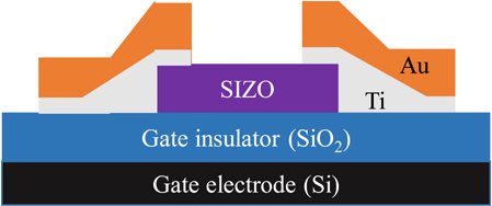
In order to create a uniform precursor of SIZO thin films, silicon tetrachloride[SiCl4], indium nitrate hydrate [In (NO3)3·xH2O], and zinc acetate dihydrate [Zn (CH3COO)2·2H2O] were mixed into a solvent of 2- methoxyethanol [C3H8O2] and ethyleneglycol, with a concentration of 0.5 M. The mole ratio of In:Zn was fixed at 1:1, and silicon was added from 0.01 to 0.4 mole. Ethyleneglycol was used as stabilizing agent to improve the solubility of precursor salts. Then, it was stirred at room temperature for 6 h to form SIZO precursor. The precursor solution was filtered through a 0.5 μm syringe filter. The solvent was then spin-coated at 3,000 rpm for 40 s on the heavily doped p-type silicon wafer. Then, it was placed on a hot plate at 300℃, in order to improve the active layer adhesion in air condition. Then, it was annealed in vacuum at 300℃ for 1h in the tube furnaces. The SIZO channel was isolated by the wet-etching process, using hydrochloric acid (HCl) for 10 sec. The width/length of active channel area was 250/50 μm. Finally, Ti/Au of 70 nm film was deposited for the source and drain electrodes by e-beam evaporator and thermal evaporator. The I-V characteristics were measured with a 4-point semiconductor analyzer, in the dark at room temperature. A diagram of the bottom-gate TFTs fabricated by the solution process in this study is shown in Fig. 1.
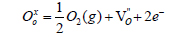
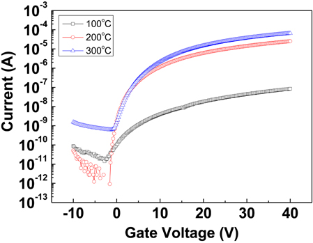
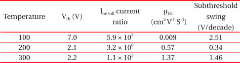
Figure 2 shows the evolution of the I-V characteristics at different process temperatures from As-grown to 300℃ of solution processed SIZO TFTs. SIZO TFTs shows the enhancement mode device. The threshold voltage was shifted toward negative direction from 7.0 to 2.2 V, when the temperature was increased. This could be explained that the annealing temperature influenced the carrier concentration, and it was not sufficient to decrease the trap state due to organic solvent and residual materials at low temperature. Consecutive post annealing under vacuum enhanced the electrical properties of the TFT, resulting in mobility from 0.009 cm2 to 1.37 V-1 s-1 cm2 V-1 s-1. The excess oxygen vacancy was generated by vacuum annealing. In the ZnO based oxides systems, free electron were generated that can improved the field effect mobility of TFT. The oxygen vacancies were generated by the following reaction:

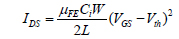
The oxygen atoms could preferentially leave their original sites. The annealing process generated the doubly charged oxygen vacancy. Oxygen vacancy could offer the carriers with two electron [11,12]. In the case of the solution processed films, it was important that the annealing temperature had generated oxygen vacancies when dehydroxylation and condensation occur. [13] The threshold voltage was determined from the conventional linear square root fitting of drain current method, and field effect mobility was calculated from the following equation.

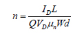
Where Ci was the capacitance per unit area of the gate insulator, W and L were the channel width and length, VGS and Vth were the gate bias and the threshold voltage, respectively. The TFT performance parameters are summarized in Table 1 with different temperature, which include the field effect mobility (μFE), the threshold voltage (Vth), the on-current (Ion), the carrier concentration, and the on-to-off current ratio (Ion/off). The electrical performance of SIZO was dependent on the annealing temperature. Field effect mobility was 1.37 cm2 V-1 s-1 for 300℃, whereas when temperature was decreased from 200 to 100℃, the field effect mobility declined from 0.57 to 0.009 cm2 V-1 s-1. The carrier concentration was calculated from the relation

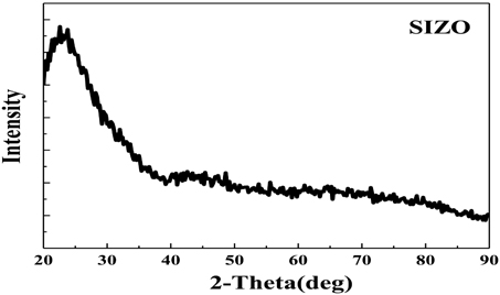
where n is the carrier concentration, ID is the measured drain current at VD = 5 V and VG = 10 V L was the gate length, W was the channel width, d was the gate insulator thickness, q was the electron charge, and μn is the electron mobility. The resulting carrier concentrations were calculated at 1016 cm-3 with increasing temperature [14]. Figure 3 shows the XRD intensity of the SIZO film at 300℃. The SIZO revealed broad peak, which clearly indicates amorphous phase. Some metal cation elements in the active channel layer make an amorphous phase or prevent their columnar growth. Therefore, the metal elements act as a diffusion suppressor of ZnO-based TFTs, because they are heavy and slow in terms of diffusion [15,16]. The SIZO TFTs with increasing annealing temperature showed enhanced field effect mobility, indicating that carrier concentration was increased.
The electrical characteristics, including threshold voltage, on-to-off ratio, μFE, and S.S of the SIZO TFTs.
We have fabricated solution processed oxide TFTs based on SIZO at an annealing temperature of 300℃ on electrical properties. When increasing annealing temperature, the formation of oxygen vacancy was increased due to generation of more electron carriers. As a result, mobility was increased, and Vth shifted toward negative direction as the annealing temperature increased.