The importance of soldering is increasing due to the rapid growth of electronic packaging industries [1-3]. Lead-containing solders (Sn-Pb) have been widely used as low temperature joining alloys because of their good combination of process attributes, convenient material properties, and low cost [4,5]. However, concerns about lead toxicity have resulted in the ban of leadcontaining solders for use in electronic devices and components [3]. Therefore, establishing a lead-free solder, such as Sn-Ag, Sn-Ag-Cu, Sn-Cu, and Sn-Zn solders has become a critical issue [6-8].
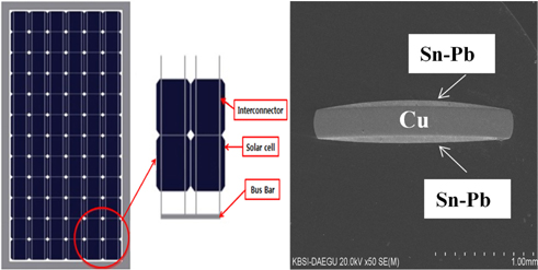
Meanwhile, a solar ribbon is widely used as an electric wire to form a connection between cells in a solar module [9], as shown in Fig. 1. Solar ribbons are generally classified into two types: interconnector and bus-bar ribbons [9]. A solar ribbon is fabricated through the solution plating of lead-containing solders (Sn-Pb) on the internal Cu ribbon [10]. The extension of a solar module’s lifespan of over 20 years is one of the most important issues in the research areas of solar ribbons [11-13]. The existence of the primary α-phases will decrease the adhesive strength between the solar ribbon and the cell, consequently decreasing the lifespan of the solar ribbon [14-16]. This study focuses on the relationship between the surface smoothness of the internal Cu ribbon and the morphology of the Sn-Pb plating layer for solar modules. The restriction of the primary α-phase's formation was enabled by enhancing the smoothness of the surface of the internal Cu ribbon.
We analyzed the interconnector and bus-bar Cu ribbon samples with products currently being used. We used the interconnector Cu ribbon, of which the thickness was about 200
The surface and cross-section morphology of the solar and Cu ribbons was observed using a scanning electron microscope (SEM; Hitach, S-4800). The composition of the surface and crosssection of the Sn-Pb plating layer was also analyzed using energy dispersive spectroscopy (EDS; Hitach, S-4800). The thickness of the Sn-Pb plating layers was measured in the cross-section SEM micrograph. The crystal structure of the Sn-Pb plating layer was analyzed by using an x-ray diffractometer (XRD; PHILIPS, X'pert APD). In addition, the adhesive strengths of pure Pb and Sn were measured using an adhesive strength tester.
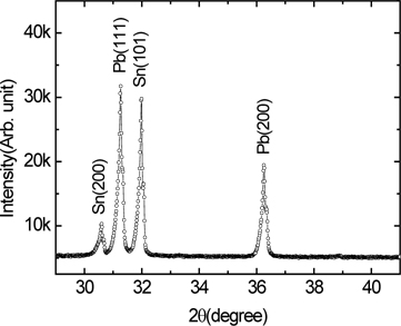
Figure 2 shows the x-ray diffraction profile of the Sn60-Pb40 (wt%) solder. We observed the crystalline Sn(200), Pb(111), Sn(101), and Pb(200) reflections. However, a Sn-Pb alloy phase was not observed. This indicates that the crystalline Sn and Pb phases in the solder existed separately.
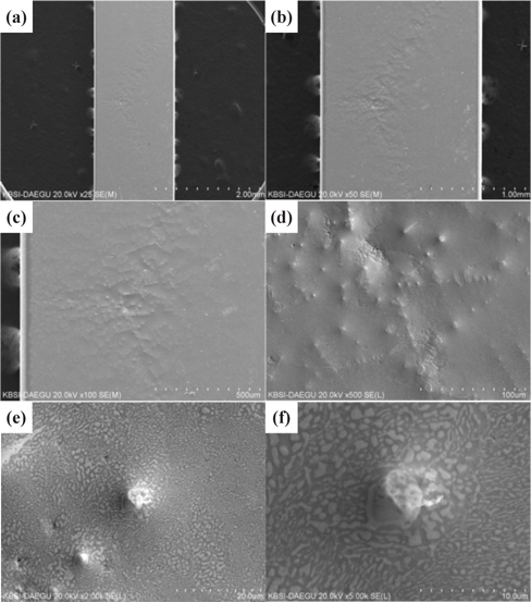
Irregular reflection of light was observed on the surface of the interconnector ribbon for solar cell modules currently being used. In order to investigate the phenomenon of the light's irregular reflection, we observed the surface morphology of the interconnector ribbons using SEM. Figure 3 shows SEM surface micrographs of the interconnector ribbon with different magnifications. Generally speaking, the irregular reflection of light is caused by a bumpy surface [17]. Irregular reflection occurs from a bumpy surface, while regular reflection occurs from a smooth surface [17]. As a result of SEM, a noticeably bumpy surface was observed on the surface of the interconnector ribbon. The irregular reflection of light occurred near the bumpy surface area of the interconnector ribbon. As shown in Fig. 3(f), large primary α-phases existed on the convex surface of the interconnector ribbon's plating layer. The diameter of the primary α-phases was about 8.5
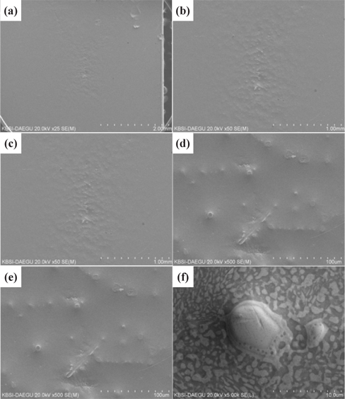
Irregular reflection of light was also observed on the surface of bus-bar ribbon for the solar cell modules currently being used Figure 4 shows SEM surface micrographs of the bus-bar ribbon with different magnifications. As a result of SEM, a noticeably bumpy surface was also observed on the surface of the bus-bar ribbon. As illustrated in Fig. 4(f), large primary α-phases existed on the convex surface of the plating layer of the bus-bar ribbon. The diameter of the primary α-phases was about 9.0
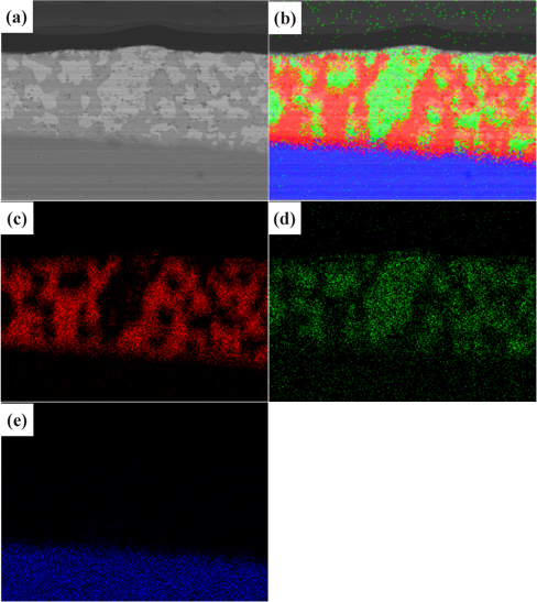
We predicted that the bumpy surface of the plating layer of the solar ribbon has a close relationship with the surface roughness of the internal Cu ribbon. In order to reveal the internal structure of the large primary α-phases, we observed the cross-sections of the interconnector ribbon by SEM. Figure 5(a) shows an SEM cross-section micrograph of the interconnector ribbon near the convex surface. We used the internal Cu ribbon, of which the thickness was about 200
It is notable that the size of the large primary α-phase in the normal direction was very similar to the plating layer's thickness. In actual practice, the nucleation rarely occurs homogeneously, but rather occurs heterogeneously on surfaces [18]. Therefore, the bumpy surface of the internal Cu ribbon is able to easily act as site for the heterogeneous nucleation of primary α-phases during the cooling of the Sn-Pb melt solutions. We considered that the primary α-phases heterogeneously nucleated on the bumpy surface of the internal Cu ribbon, and then largely grew to the surface of the Sn-Pb plating layer [18].
Figure 5(b) shows the EDS cross-section mapping images of the composition of a interconnector ribbon, which was acquired from the SEM cross-section micrograph of Fig. 5(a). The compositions of Sn, Pb, and Cu (red, green, and blue, respectively) are shown in Figs. 5(c), 5(d), and 5(e). As shown in Fig. 5(d), the large primary α-phase is clearly a Pb-rich phase. This result is consistent with the theoretical composition of primary α-phase, 19.2 wt% Sn-80.8 wt% Pb [19,20]. The melting temperature of Pb, 327℃, is 95℃ higher than that of Sn, 232℃, and is 144℃ higher than that of the eutectic temperature of Sn-Pb, 183℃ [19, 20]. The eutectic structure is composed of a eutectic α-phase and β-phase, and the eutectic composition is 61.9 wt% Sn-38.1 wt% Pb [19,20]. The large, Pb-rich, primary α-phases can cause a decrease of the adhesive strength between the ribbon and cell, compared to that of the eutectic structure. The adhesive strength of pure Pb was very small at 81 N/mm2, compared to that of pure Sn, 218 N/mm2. Also, the resistivity of pure Pb was very large at 208 nΩ·m, compared to that of pure Sn, 115 nΩ·m. Therefore, the existence of the large primary α-phases can significantly reduce the lifespan and increase the contact resistance of the Cu ribbon for solar modules.
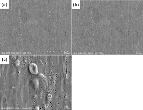
In order to confirm the existence of the bumpy surface of the internal Cu ribbon, we carefully observed the surface morphology of the Cu ribbon. Figure 6 shows the SEM surface micrographs of pure Cu ribbon for solar cell modules currently being used, with different magnifications. As a result of SEM, a bumpy surface with convex parts was observed on the surface of the pure Cu ribbon. As illustrated in Fig. 6(c), the diameter of the convex parts of the surface of the pure Cu ribbon was about 2~5
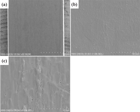
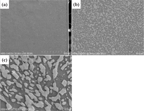
We have enhanced the smoothness of pure Cu ribbon by improving the surface smoothness of the press roller during the calendering of Cu wire. We also chose a Cu wire that has an excellent surface smoothness. Figure 7 shows SEM surface micrographs of pure Cu ribbon having enhanced smoothness with different magnifications. As a result of SEM, we could observe the internal Cu ribbon's smooth surface with almost no convex parts.
With the internal pure Cu ribbon having enhanced smoothness, we fabricated the interconnector ribbon in the same condition. Figure 8 shows the SEM surface micrographs of the interconnector ribbon with different magnifications. After Sn-Pb plating on the smooth internal Cu ribbon, the surface smoothness of the interconnector ribbon was improved by restricting the formation of the large primary α-phases. We confirmed that the solar ribbon's surface smoothness depends on the internal Cu ribbon's surface smoothness.
We studied the relationship between the surface smoothness of a Cu ribbon and the surface/cross-section morphology of a Sn-Pb plating layer for solar modules. From the result of SEM, a bumpy surface was observed on the surface of the solar ribbon, which caused irregular reflection of light. Large, Pb-rich, primary α-phases were found below the convex surface of the solar ribbon, passing from the surface of the internal Cu ribbon to the surface of the Sn-Pb plating layer. The size of the large primary α-phase in the normal direction was about 15