(111)-oriented and random oriented Pb0.8Ba0.2ZrO3 (PBZ) perovskite relaxor ferroelectric thin films were fabricated on Pt(111)/TiOx/SiO2/Si substrate by sol-gel method. Nano-scaled antiferroelectric and ferroelectric two-phase coexisted in both (111)-oriented and random oriented PBZ thin film. High dielectric tunability (η=75%, E = 560 kV/cm) and figure-of-merit (FOM ~ 236) at room temperature was obtained in (111)-oriented thin film. Meanwhile, giant electrocaloric effect (ECE) (ΔT=45.3K and ΔS=46.9JK−1kg−1 at 598kVcm−1) at room temperature (290 K), rather than at its Curie temperature (408 K), was observed in random oriented Pb0.8Ba0.2ZrO3 (PBZ) thin film, which makes it a promising material for the application to cooling systems near room temperature. The giant ECE as well as high dielectric tunability are attributed to the coexistence of AFE and FE phases and field-induced nano-scaled AFE to FE phase transition.
Dielectic tunable materials have recently received renewal attention due to the potential applications in filters, phase shifters, wireless communications, etc. [1,2]. These applications demand dielectric materials to possess not only the high dielectric tunability, but also the low dielectric loss, high figure-of-merit, and high temperature stability [3,4]. To accomplish these requirements, most research efforts in this area are mainly focused on investigating the titanium-containing perovskite ferroelectric materials such as (Ba,Sr)TiO3 (BST), Ba(Zr,Ti)O3 (BZT), etc. [5,6]. Due to the oxidation state of titanium being easily reduced from Ti4+ to Ti3+, [7-12] the dielectric tunable properties of these titanium-containing ferroelectrics usually undergo degradation (dielectric loss increasing and figure-of-merit decreasing) at high temperature.
ECE is a change in temperature (ΔT) in a polarable material by virtue of the change in entropy (ΔS) upon the application or withdrawal of an electric field under adiabatic conditions [13-15]. Simulation results [16] indicate that cooling devices based on large ECE can have much higher coefficient of performance (COP) (> 60% of Carnot efficient) than those (< 20% of Carnot efficient) of mechanical vapor compression cycle cooling devices such as refrigerator and air-conditioner, which generate strong greenhouse gases during their operations. For the development of ECE cooling technologies in the past, the bottle neck [17] existed because only a small ΔT and ΔS can be induced in bulk materials, such as only ΔT = 2.5 K and ΔS = 0.2 JK−1kg−1 at 750 V in Pb0.99Nb0.02(Zr0.75Sn0.20Ti0.05)O3 ceramics, due to the restriction of breakdown fields (~ 50 kVcm−1). By resorting to a thin-film geometry, giant ECE (ΔT = 12 K and ΔS = 8 JK−1kg−1 at 776 kVcm−1) in the antiferroelectric PbZr0.95Ti0.05O3 (PZT) was observed by Mischenko et al. [13] in near antiferroelectric to paraelectric phase transition temperature (Tc = 500 K). This has triggered a new wave of interest in the search for new ECE materials, which resulted in significant progress in this field and raised hope for successful development of ECE solid-state cooling units. For example, Saranaya et al. [18] reported a bigger ECE temperature change (ΔT = 31 K) at 413 K and 747 kVcm−1 in Pb(Mg1/3Nb2/3)0.65Ti0.35O3 thin films deposited by PLD. But the application of cooling devices needs maximum EC effect at or near room temperature.
In this work, (111)-oriented and random oriented nano-scaled antiferroelectric and ferroelectric two-phase coexisting in relaxor Pb0.8Ba0.2ZrO3 thin film were fabricated by a sol-gel method. High temperature stability (η > 75% and FOM > 230 at 560 kV/cm in the range from 300 K to 380 K) was achieved in the (111)-oriented PBZ thin film, making this thin film comparable with those titanium-containing ferroelectric materials. Meanwhile, a giant ECE (ΔT = 45.3 K and ΔS = 46.9 JK−1kg−1 at 598 kVcm−1) in the random oriented Pb0.8Ba0.2ZrO3 thin film at room temperature (290 K), away from its Curie temperature (408 K), was observed.
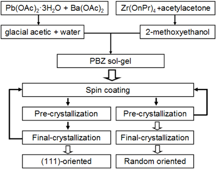
Pb80Ba20ZrO3 (PBZ) thin films were fabricated by a sol-gel method. Pb(OAc)2·3H2O and Ba(OAc)2 were dissolved in glacial acetic and deionized water. In order to compensate for the Pb loss during sintering, 20% of excess Pb was added. Separately, acetylacetone was added to a mixture of Zr(On Pr)4 and 2-methoxyethanol, and the resulting solution was stirred for 30 min at room temperature. The Pb/Ba and Zr solutions were then mixed and stirred for 2 h at room temperature. The final concentration of the synthesized PBZ sol was 0.3 M. After aging the sol for 24 h, the PBZ sol was passed through a 0.2 μm filter and spun onto Pt(111)/TiOx/SiO2/Si(100) substrates at 4,000 rpm for 30 s. The substrates were rinsed with acetone and 1-propanol before use. To obtain the (111)-oriented PBZ thin film, each layer was pyrolized at 350℃ for 3 min and then heated at 550℃ for 3 min on hotplates, and finally annealed at 800℃ for 3 min in a tube furnace in air.
The above-mentioned procedure was repeated 8 times to obtain the desired thickness. To obtain the random oriented PBZ thin film, each layer was pyrolized at 350℃ for 3 min and then heated at 550℃ for 5 min on hotplates. After the deposition of 8 layers, the film was annealed in a tube furnace at 750℃ for 30 min in air. To be clear, Fig.1 shows the above preparation process of two different Pb0.8Ba0.2ZrO3 thin films. The final thicknesses for all of the films were about 320 nm. Cr/Au top electrodes of 150 μm diameter were evaporated through a patterned photoresist mask. The structure of the PBZ films were monitored by X-ray diffraction (XRD; Bruker-AXS D5005, Siemens, Munich, Germany) on a diffractometer, using Cu Kα radiation (λ=1.5406 Å). The cross-sectional and surface morphologies of the film were examined by scanning electron microscope (SEM; FEI XL30 SFEG, Philips, Eindhoven, The Netherlands). Dielectric permittivity measurements were carried out using an impedance analyzer (Wayne-Kerr Electronics, West Sussex, UK) at V = 100 mV. Electric field dependences of polarization hysteresis (PE) loop and leakage current (I(t)) were obtained by means of a ferroelectric tester (RT66A, Radiant Technologies Inc., Albuquerque, NM, USA). The temperature of the sample was controlled via feedback from a thermocouple, accurate to 0.1℃, in contact with the sample.
Superlattice reflections with indices (130)/(112) and (014) in XRD patterns indicate the existence of orthorhombic antiferro-electric phase both in the (111)-oriented and random oriented PBZ thin film. The SEM surface images further revealed that the microstructure of the two PBZ thin films were uniform, homogeneous, and crack-free, with average grain size of 20 nm. To further study the morphology and microstructure of the two PBZ thin films in detail, the TEM characterization was carried out.
Numerous dispersed nanocrystals corresponding to those subgrains in the SEM were observed in the TEM bright field images. Inside of some nanocrystals, lamellar nanodomains with about 2 nm of width and lamellar nanodomains with about 1 nm of width were clearly visible. The latter can be attributed to the antiferroelectric domains with 1 nm of width close to its cell parameters, which is consistent with the report by Viehland in PZT. [19] According to the refined α values (90.9463°) of the RFE (rhombohedral ferreoelectric) phase and the feature of the SAED patterns in the two PBZ thin films, lamellar nanodomains with about 2 nm of width probably are due to the existence of 180° ferroelectric domains.
Typical characteristic of ferroelectric relaxor was observed around the dielectric permittivity peak of the temperature dependences of dielectric permittivity (ε) of the two PBZ thin films. In contrast, the same character was detected in Pb(1−x) BaxZrO3 bulk ceramics with Ba2+ substitution at x < 0.3. [20] This difference can be attributed to the mismatch effect between the film and the substrate and to the smaller grain size. Although the dielectric permittivity (see Table 1) was higher compared with those found in PZT-based compositions, it was rather lower than that obtained in the corresponding sintered bulk PBZ ceramics with the same composition, which may most probably be due to the limited film thickness. Likewise, the maximum dielectric permittivities were observed at 433 K (Tm at 100 Hz) in (111)-oriented thin film and at 408 K (Tm) in random oriented thin film, rather than at 425 K as reported with PBZ bulk material. The antiferroelectric to ferroelectric (AFE-FE) phase transition in the (111)-oriented thin film was detected at 354 K, which was also observed on the P-T (polarization vs temperature) curve plotted from the P-E (polarization vs electric field) loops at 10 kHz and 156 kV/cm. In contrast, the AFE-FE phase transition in the random oriented thin film was not obviously detected.
[Table 1] Dielectric and filed-induced electrical properties of Pb0.8Ba0.2ZrO3 thin films.
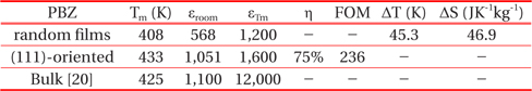
Dielectric and filed-induced electrical properties of Pb0.8Ba0.2ZrO3 thin films.
Dielectric tunability (η) and figure-of-merit (FOM) of the (111)-oriented PBZ thin film at 10 kHz at room temperature can be defined as follows:


where ε(0) and ε(E) represent the dielectric permittivity at zero and a certain electric field, respectively. It was found that the tunability increased with E, and 75% of tunability was achieved at E = 560 kV/cm in both polarizing and depolarizing branches. Similar to tunability, FOM also increased with E and a maximum value of 236 was obtained, indicating that the PBZ thin film can be a very promising material for applications to dielectric tunable device.
For a competent dielectric tunable material, not only high value of tunability and high Figure-of-merit are required, but also the high temperature stability is necessary. With the increase of the temperature, the tenability of the (111)-oriented PBZ thin film first increased and reached a maximum (about 84%) at 430 K, close to the Tm, and then decreased. Different from the tunability, the maximum FOM (about 268) was observed at 345 K, close to the TAFE-FE, which can be ascribed to the smaller dielectric loss at TAFE-FE. These results indicate the high temperature stability of tunable property of the (111)-oriented PBZ thin film. These are desired for the application of tunable devices, because the FOM and tunability for dielectrics that are used in their paraelectric state usually tend to deteriorate during the operations, caused by a rise of temperature, especially for the titanium-containing dielectric materials.
Assuming the Maxwell relation (∂P/∂T)E = (∂S/∂E)T, reversible adiabatic changes in temperature (ΔT) and entropy (ΔS) for the random oriented PBZ thin film can be calculated by [13-15]
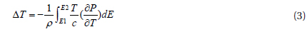
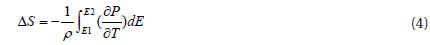
where ρ is the density, and C is the heat capacity. Values of (∂P/∂T)E were obtained from four-order polynomial fits to the cubic-spline interpolation of raw P(T) data, extracted from the upper branches of P-E loops in E > 0. In the temperature range of interest, the heat capacity (C = 330 JK−1kg−1) remains constant for Zr-rich, lead-based thin film [13]. The theoretical density ρ of PBZ thin film with the pseudocubic structure was determined to be 7.7 gcm-3 from the XRD pattern, by using the software JADE. Using Eq. (1) and Eq. (2), the ΔT and ΔS of the random oriented thin film at selected electric fields were obtained. Peak ΔT = 45.3℃ at 598 kVcm−1 was obtained at 290 K, as well as peak ΔS = 46.9 JK−1kg−1.
In order to elucidate the giant ECE in the random oriented PBZ thin film, the pyroelectric coefficients (∂P/∂T)E at selected electric fields were plotted. With the increase of the electric field, the (∂P/∂T)E at around the temperature of the peak first increased and reached a maximum at 210 kVcm−1, and then decreased. Likewise, the (∂P/∂T)E near and between the temperature of the twin-peak first increased and reached a maximum at 100 kVcm−1, and then decreased.
To get an insight into this phenomenon, P-E loops under different electric fields and the dc electric field dependence of the permittivity (ε(E)) were investigated at 293 K and 403 K. Double P-E loops were visible at 293 K when the electric field was lower than 210 kVcm−1, indicating that an electric field induced AFE-FE phase transition was taking place. Typical ferroelectric P-E loops were obtained when the electric field was higher than 210 kVcm−1. In contrast, only ferroelectric P-E loops were obtained at 403 K under all electric fields. A peak in the curve of ε(E) was observed at 293 K, which further revealed the existence of the electric field induced AFE-FE phase transition. No peak was detected in the curve of ε(E) at 403 K. In summary, it can be inferred that the giant EC at room temperature for PBZ thin film may be caused by the electric field-induced AFE-FE phase transition, which could induce new ways to enhance the electrocaloric efficiency by virtue of the noncollinearity between the electric field and the polarization. It is well known that for second order phase transition or higher order phase transition, the entropy change ΔS is normally smaller than first order phase transition. Bhadra et al. [21] carried out a high temperature X-ray study of structure phase transitions in Pb1−xBaxZrO3 powders and confirmed the first order nature of the AO to FR transition. The AO to FR transition is similar to the austensite (A) to martensite (M) transition in some alloys, and large ΔS can be caused during the transition. Previous work [22,23] pointed out that latent heat (or ΔS) from the field-induced phase transition can significantly contribute to the ECE below the depolarization temperature Tdp. Therefore, the giant ECE at room temperature as well as the high dielectric tunability for PBZ thin film can be attributed to the contribution of the electric field inducing AO to FR transition [24,25].
(111)-oriented and random oriented nano-scaled antiferroelectric and ferroelectric phases coexisting relaxor Pb0.8Ba0.2ZrO3 thin film were successfully prepared by a sol-gel method. A high dielectric tunability (η ~ 75%), figure-of-merit (FOM ~ 236), temperature stability (η > 75% and FOM > 230 at 560 kV/cm in the range from 300 K to 380 K), and high dielectric strength (leakage current < 1 nA at 598 kV/cm) were observed in the (111)-oriented PBZ thin film, which make it a promising material for applications of tunable devices. A giant ECE (ΔT = 45.3 K and ΔS = 46.9 JK−1kg−1 at 598 kVcm−1) at room temperature (290 K), rather than at the Curie temperature (408 K), was obtained in the random oriented Pb0.8Ba0.2ZrO3 thin film. This makes it usable as a promising material for applications in cooling systems near room temperature. Field-induced, nano-scaled antiferroelectric to ferroelectric phase transition played a key role in the dramatic EC effect.