The design of a new compact band-pass filter is proposed, which is based on the microstrip composite right- and left-handed transmission-line (CRLH-TL) structure. Particularly, the interdigital coupled (IDC) lines of the CRLH geometry are proposed to be parted by inserting open stubs to meet the specifications on the passband. In addition, there is another pair of stubs to complete the design in a limited space. These are considered in the TL-based analysis and the design parameters are calculated by genetic algorithm optimization. The measurement is shown to be acceptable and agreeable with the circuit and electromagnetic field simulations. In addition, the zerothorder resonance (ZOR) phenomenon is verified.
In recent years, numerous studies have been conducted to exploit the benefits of broadband communication since LTE service began to enable carriers and terminals to transmit and receive hundreds of Mbps of data, as well as to step forward to realize a Gbps data transmission would lead to 5G services. As one of many such research activities, the methods of designing band-pass filters (BPFs) have been reported to keep abreast of evolving wireless communication systems equipped with multifunction antennas and circuitry as well [1-5].
Ishida and Araki [1] designed a very wide-band BPF whose bandwidth is formed by adding zeros in the sections of the transmission line (TL). Its frequency response has notches only at the band edges and has an extremely narrow stopband. Wang et al. [2] presented the microstrip-and-CPW BPF for broadband applications, which is based on the multi-mode resonator (MMR) in the form of multiples of a quarter wavelength to broaden the bandwidth and obtain an enlarged rejection region. The idea of the MMR of the half wavelength is also used in [3], where the coupled lines of a quarter wavelength are used as the inverter. This work demonstrates the extension of the lower and higher stopbands owing to increased coupling. A composite wide-band filter was designed by Menzel et al. [4] by combining low- and high-pass filters as suspended stripline structures with different planes. Independently, Hsu et al. [5] presented composite microstrip filters for high-speed communication applications, where seven or eight TL sections of about a quarter wavelength are sequentially connected.
Recently, we suggested the design of a novel wide-band filter based on the composite right- and left-handed transmission line (CRLH-TL) metamaterial [6]. Contrary to the reference [6], we propose the use of one segment (smaller than one quarter wavelength) to make the component very compact. Besides, instead of mixing two types, for instance, as a hybrid of the microstrip and CPW, we use only the microstrip whose fabrication is inexpensive. Especially, in our proposed CRLH BPF geometry, we separate the interdigital coupled (IDC) lines by inserting open stubs between and grounded stubs to form a 1.7-GHz bandwidth. Furthermore, out of the CRLH unit, we place another pair of open stubs to improve the passband performance. The proposed filter, whose size is less than 1 × 1 cm2, is fabricated and measured to be proven acceptable for the specifications.
II. DESIGN OF THE CRLH-TL TYPE UWB BPF
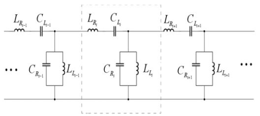
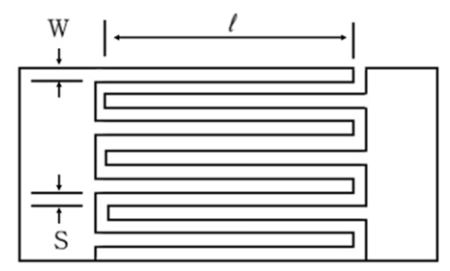
The conventional CRLH-TL is a periodic structure with multi-cells, as shown in Fig. 1 [6]. The
The lumped elements of the 1-cell CRLH-TL are obtained to generate a center frequency

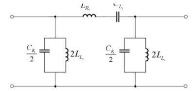
Although, we use the Fig. 2 circuit, as it will change in the physical implementation, and we propose a new and hybridphysical geometry, which will be explained later.
As it comprises the lumped elements and TL seg-ments, it is called a hybrid-physical circuit. The values of the CRLH-TL BPF with open stubs are calculated as follows to achieve the objectives in Table 1A.
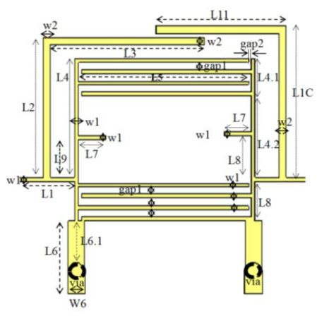
Fig. 2 is related to Fig. 3 through the pi-shaped IDC lines flanked with shorted stubs appearing in [7,8]. One block of the IDC lines is equally divided into the upper and lower blocks of the IDC lines (represented by
[Table 1A.] Design goal of this filter: lower half of the UWB

Design goal of this filter: lower half of the UWB
[Table 1B.] Initial values of the elements for the circuit above

Initial values of the elements for the circuit above
Even if the IDC line has been around for some time, as stated before, its geometric parameters will be explored to find the desired effective inductance
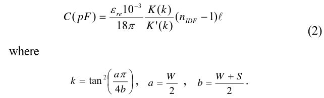
The expression as follows is commonly used for the inductance of Fig. 6 (
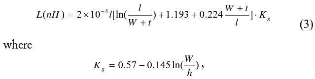
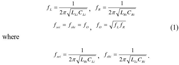
where
[Table 2.] Initial values of the elements of the proposed geometry
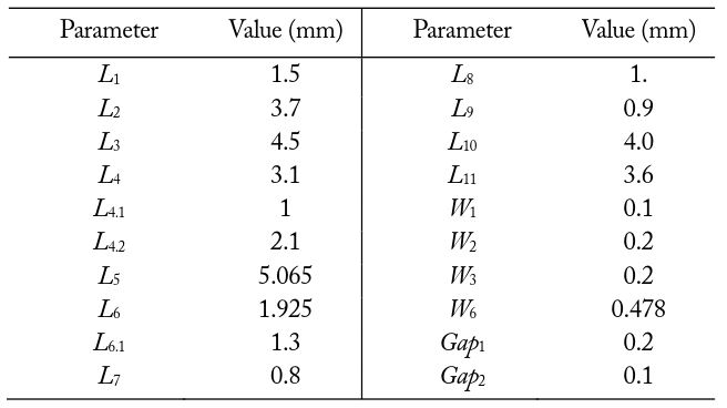
Initial values of the elements of the proposed geometry
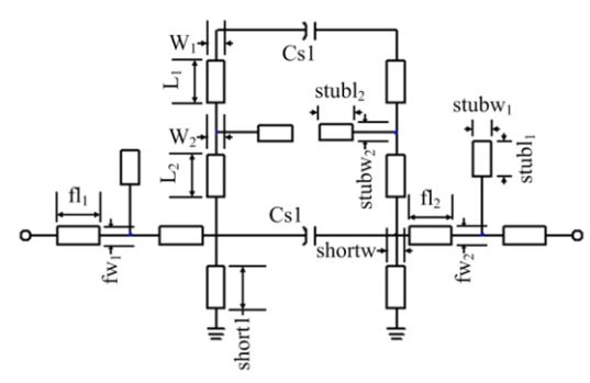
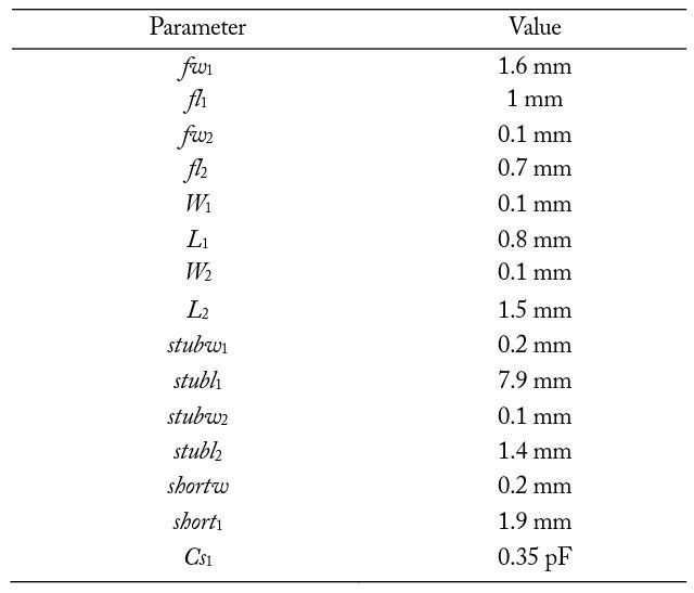
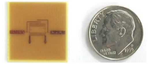
First, the interdigital capacitor’s size is calculated to realize a capacitance of 0.35 pF. As a result, the finalized geometry and all its physical dimensions are shown in Fig. 7 and Table 2.
With the structure above, we use FR4 (
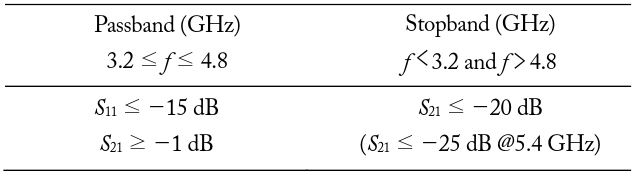
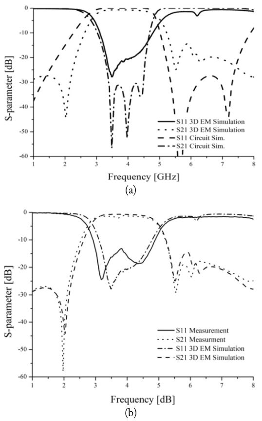
Fig. 8 plots the circuit and 3D field-simulated scattering parameters
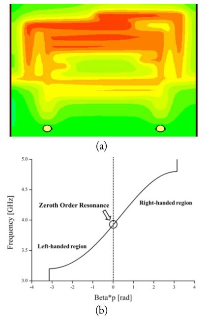
As the basis of our proposed geometry is the CRLH-TL, the metamateial property can be proven by watching the electric field and the dispersion diagram (or propagation constant vs. frequency diagram). Fig. 9(a) shows the ZOR phenomenon at
As in Figs. 7 and 10, our filter fits into the 1 × 1 cm2 area and is less than even a quarter wavelength in area (1.83 × 1.83 cm2), which means 54%- and greater than 70%-size reductions from the conventional quarter wavelength and half wavelength, respectively. In addition, we compared our filter with other size-reduced broadband structures to present the differences, features, and advantages of the proposed method.
Based on the comparison in Table 3, our structure is the shortest due to the use of the ZOR effect, which helps our design to have an insertion loss below 1 dB. In addition, it is easier to fabricate our filter compared to the defected ground in [2] and the multi-layers and metal housing in [4] now that ours is manufacturable as a printed 1-layer planar geometry.
[Table 3.] Comparison between our and other broadband filters
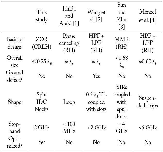
Comparison between our and other broadband filters
A new compact UWB lower-half BPF has been proposed based upon the concept of the CRLH-TL metamaterial. Only one unit of the CRLH-TL is adopted and the two pairs of inner and outer open stubs are added to form the wanted passband. After a 3D electromagnetic field simulation and fabrication, the design is validated by the measurement to show an excellent performance of the frequency response with a 3.2–4.8 GHz band, a less than 1-dB insertion loss and a less than 15-dB return loss. Lastly, the proposed design makes the overall size of the filter less than 1 × 1 cm2 in area.