The demand is currently increasing for small-cell base stations, such as pico-cell and femto-cell to improve system caacity and flexibility. The power amplifier (PA) in small-cell base stations consumes a large portion of the system power and volume. Therefore, the PA should be efficient and small.
A linear amplification of the high peak-to-average power ratio (PAPR) signal should be achieved by operating the PA for the system in a large back-off output power region, where the PA shows a poor efficiency. The efficiency around the average output power level has been enhanced by the introduction of several efficiency enhancement techniques have been introduced, such as envelope elimination and restoration (EER), envelope tracking (ET), and Doherty power amplifier (DPA) techniques [1–4]. Among these techniques, DPA, which employs a load impedance modulation technique, has been widely used in the base station due to its simple structure and high efficiency at the average output power region.
The DPA is usually implemented with a hybrid configuration in the base stations. In the hybrid PA, the matching network is too large to be useful for the small-cell base station. A limitation also exists on selecting the sizes of the carrier and peaking cells for the DPA due to the device availability. For these reasons, we design a DPA using monolithic microwave integrated circuit (MMIC) process to get a small size and proper cell size ratio of the carrier and peaking PAs for an optimized operation [5,6]. The highest efficiency for a LTE signal with 7.2-dB PAPR is obtained by applying an asymmetric Doherty structure [7,8].
The digital predistortion (DPD) technique is widely used for the base station to linearize the PA. However, the DPD circuit board consumes a lot of power for the small-cell base station. Therefore, the DPA should have high linearity in order to linearize the PA using a light PD system. To get a high linearity, third-order inter-modulation (IM3) cancellation method is applied for the Doherty structure [9,10]. In this paper, the detailed circuit design of the highly efficient and linear DPA is presented in Section II, followed by the simulation and experimental results of the PA in Section III.
II. HIGHLY EFFICIENT AND LINEAR ASYMMETRIC DOHERTY POWER AMPLIFIER
For the base station application, the DPA is usually designed in a hybrid configuration consisting of discrete power cells and distributed passive elements. The hybrid configuration is not an appropriate structure fora small-cell base station because it occupies a large area. Selection is also limited for the device sizes of the carrier and peaking PAs due to device availability.
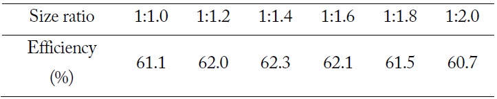
However, no limitation exists for the MMIC with respect to selection of the sizes of the carrier and peaking PAs. We obtained a high efficiency for amplification of the LTE signal with 7.2-dB PAPR by calculating the efficiency for an ideal asymmetric DPA with different cell size ratio of the carrier and peaking PAs from 1:0.8 to 1:2.0. From the ideal simulation result, we find that a 1:1.4 cell size ratio provides the highest efficiency, which is a 1.2% higher average efficiency than a symmetric structure, as shown in Table 1. Therefore, we design the DPA with 1:1.4 cell size ratio for a good efficiency performance.

The efficiency of the asymmetric Doherty power amplifier (DPA) for the LTE signal according to the size ratio of the carrier and peaking PAs
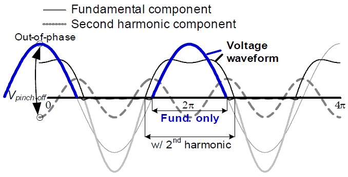
Fig. 1 shows the input voltage waveform of the PA with and without the second harmonic short circuit at the input.
Due to the nonlinear input capacitor [11], the second harmonic of the input voltage is out-of-phase with the fundamental component. The out-of-phase second harmonic component increases the conduction angle of the input voltage waveform, as shown in Fig. 1. The increased conduction angle results in a larger DC component for the current waveform, which degrades the efficiency of the PA. The efficiency is enhanced by inserting the second harmonic short circuit at the input of the carrier PA. However, in the case of the peaking PA, the matching concept should be different. It has a lower output power due to the class C-bias and this lower output power leads to the improper load modulation of the DPA. Therefore, the second harmonic short circuit is not inserted at the input of peaking PA to get the additional output power needed for proper load modulation.
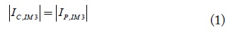
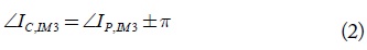
The DPD technique is widely used the base station to linearize the PA. However, the DPD circuit board consumes too much power to be useful for the small-cell base station. Therefore, one solution could be a light PD system that consumes less DC power. However, the linearization capability of the light PD system is limited and the DPA should have high linearity. The linearity of the DPA can be improved by cancelling out the IM3s of the carrier and peaking the amplifier sat the output combining point. The gain compression characteristics of a class AB carrier PA and the gain expansion of the class C peaking PA make it possible to cancel them. When the IM3 characteristics of the amplifiers are perfectly satisfied with the Eqs. (1) and (2), the IM3s are cancelled out maximally at the output combining point of the Doherty topology,


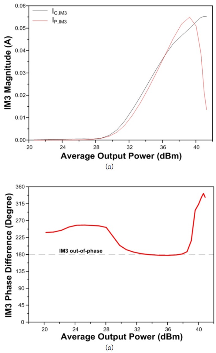
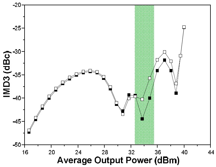
Fig. 2 shows the magnitude and phase differences between IC,IM3 and IP,IM3 according to the output power. The simulation result shows that the Eqs. (1) and (2) are satisfied near 34 dBm output power region. Fig. 3 shows the two-tone IMD 3 curves of the proposed DPA. Employing the IM3 cancellation method gives an IMD3 under 35 dBc near the output power of 34 dBm.
III. SIMULATED AND EXPERIMENTAL RESULTS
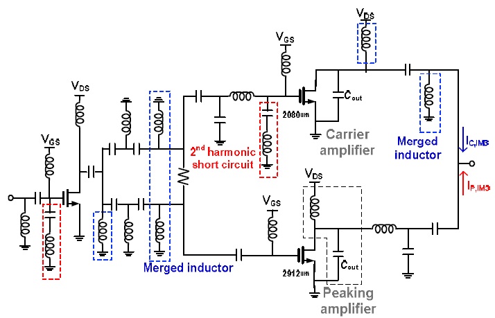
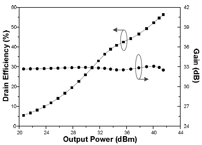
The design concept is validated by designing a highly linear 2-stage DPA using Agilent Advanced Design System. An overall schematic of the linear asymmetric 2-stage DPA is shown in Fig. 4. The total gate width of the drive PA, carrier PA, and peaking PA are 560 μm, 2,080 μm, and 2,912 μm, respectively. The second harmonic short circuit and merged inductor are adopted for a high efficiency and small size. The IM3 cancellation method is applied for a high linearity. For the simulation, the drain bias voltages of the drive PA, carrier PA, and peaking PA are set to 20 V, 28 V, and 28 V, respectively. The quiescent current of the drive PA and carrier PA are set to the class-AB bias with 28 mA and 160 mA, respectively. Fig. 5 shows the simulated performances of the 2-stage DPA for a 2.14-GHz CW signal. The simulated drain efficiency and gain at 7.2 dB back-off power level are more than 40.0% and 32.5 dB, respectively, and the peak output power is over 41 dBm.
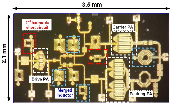
The proposed asymmetric 2-stage DPA is validated by realizing the PA using TriQuint 3MI 0.25-μm GaN-HEMT MMIC process. The integrated circuit size, except for the RF choke inductor, is only 3.5 mm × 2.1 mm as shown in Fig. 6.
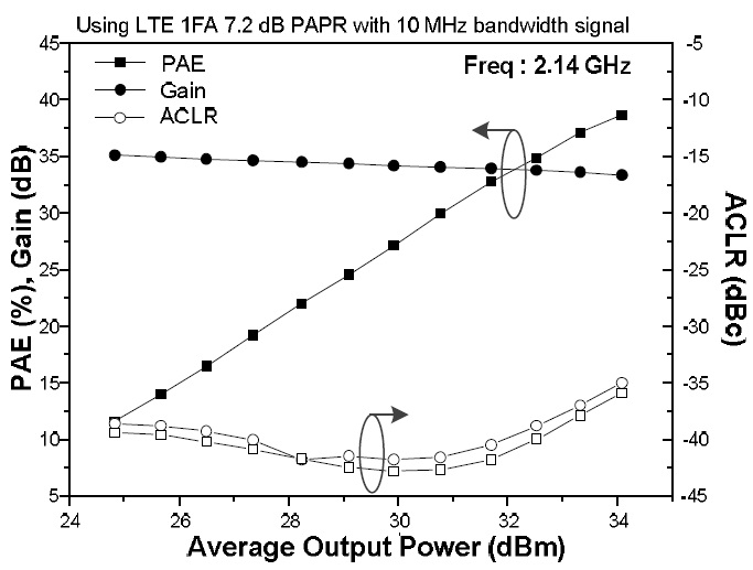
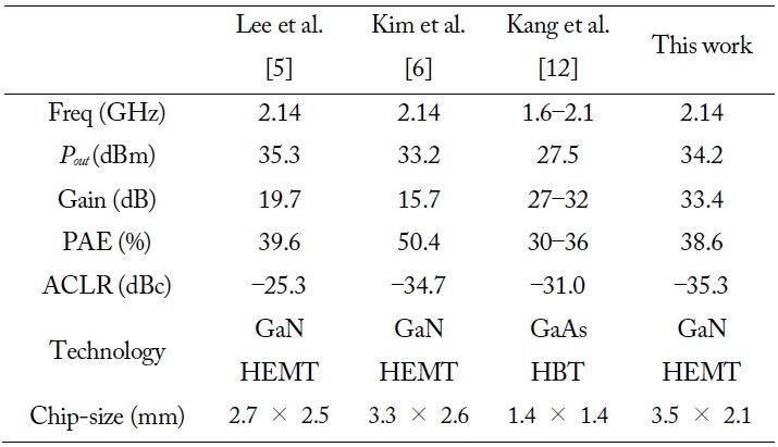
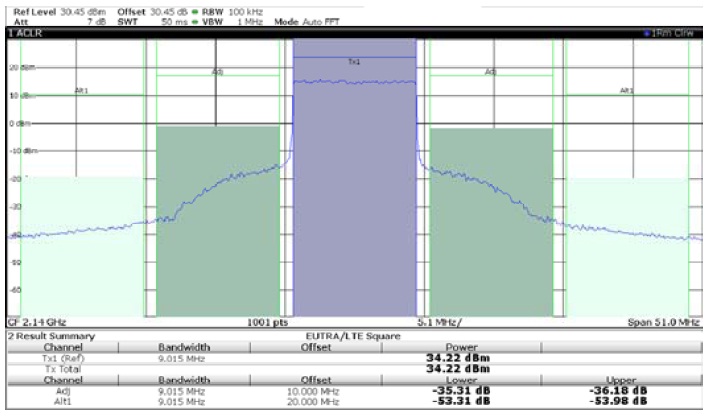
For the experiment, drain bias voltages of the drive PA, carrier PA, and peaking PA are set to 20 V, 28 V, and 28 V, respectively. The quiescent currents of the drive PA and carrier PA are 28 mA and 160 mA, respectively, class-AB biases. The high efficiency and linearity of the asymmetric DPA for the modulated signal is validated by testing the PA using an LTE signal with 10-MHz bandwidth and 7.2-dB PAPR at 2.14 GHz. Fig. 7 shows the measured efficiency, gain, and adjacent channel leakage ratio (ACLR) characteristics. The implemented 2-stage DPA delivers the power-added efficiency (PAE) of 38.6%, a gain of 33.4 dB, and ALCR of –35.3 dBc at an average power of 34.2 dBm. Fig. 8 shows the measured output spectra of the proposed DPA at an average output power of 34.2 dBm. From the output spectra, we can recognize the high linear characteristic of the proposed DPA. For comparison, the performances of the recently reported MMIC PAs are summarized in Table 2. The linearity and efficiency of the proposed DPA is favorable among the reported Pas for smallcell base station systems.
[Table 2.] Performance comparison of recently reported MMIC DPA

Performance comparison of recently reported MMIC DPA
An asymmetric DPA based on GaN HEMT MMIC process is designed and fabricated for a small-cell base stations. The highest efficiency for 7.2-dB PAPR LTE signal is obtained with the asymmetric DPA which has 1:1.4 cell size ratio for the carrier and peaking PAs is designed. A higher efficiency is obtained by inserting a second harmonic control circuit at the carrier PA. The operation is highly linear when the IM3 cancellation method is applied. With this design concept, the asymmetric DPA is implemented using the TriQuint 3MI 0.25-μm GaN-HEMT MMIC process. At 2.14 GHz, the implemented PA delivers a PAE of 38.6%, a gain of 33.4 dB, and an ACLR of –35.3 dBc at an average power of 34.2 dBm for LTE signal with a 7.2-dB PAPR.